- 您現在的位置:買賣IC網 > PDF目錄374046 > ADV7181BBCPZ (ANALOG DEVICES INC) Multiformat SDTV Video Decoder PDF資料下載
參數資料
| 型號: | ADV7181BBCPZ |
| 廠商: | ANALOG DEVICES INC |
| 元件分類: | 顏色信號轉換 |
| 英文描述: | Multiformat SDTV Video Decoder |
| 中文描述: | COLOR SIGNAL DECODER, QCC64 |
| 封裝: | 9 X 9 MM, LEAD FREE, MO-220-VMMD, LFCSP-64 |
| 文件頁數: | 12/96頁 |
| 文件大小: | 873K |
| 代理商: | ADV7181BBCPZ |
第1頁第2頁第3頁第4頁第5頁第6頁第7頁第8頁第9頁第10頁第11頁當前第12頁第13頁第14頁第15頁第16頁第17頁第18頁第19頁第20頁第21頁第22頁第23頁第24頁第25頁第26頁第27頁第28頁第29頁第30頁第31頁第32頁第33頁第34頁第35頁第36頁第37頁第38頁第39頁第40頁第41頁第42頁第43頁第44頁第45頁第46頁第47頁第48頁第49頁第50頁第51頁第52頁第53頁第54頁第55頁第56頁第57頁第58頁第59頁第60頁第61頁第62頁第63頁第64頁第65頁第66頁第67頁第68頁第69頁第70頁第71頁第72頁第73頁第74頁第75頁第76頁第77頁第78頁第79頁第80頁第81頁第82頁第83頁第84頁第85頁第86頁第87頁第88頁第89頁第90頁第91頁第92頁第93頁第94頁第95頁第96頁
ADV7181B
ANALOG FRONT END
Rev. 0 | Page 12 of 96
0
AIN2
AIN1
AIN4
AIN3
AIN6
AIN5
A
A
A
A
A
A
AIN4
AIN3
AIN6
AIN5
AIN6
AIN5
ADC_SW_MAN_EN
ADC0_SW[3:0]
ADC1_SW[3:0]
ADC0_SW[3:0]
ADC2
ADC1
ADC0
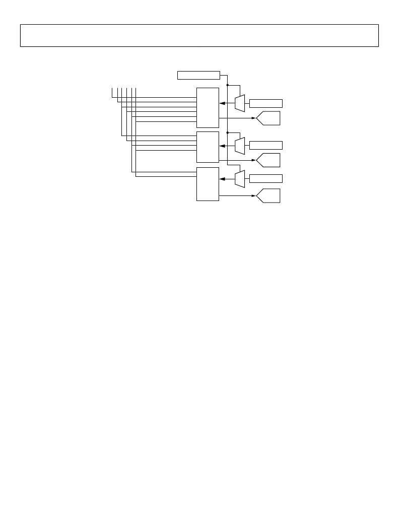
Figure 5. Internal Pin Connections
There are two key steps to configure the ADV7181B to correctly
decode the input video.
1.
The analog input muxing section must be configured to
correctly route the video from the analog input pins to the
correct set of ADCs.
2.
The standard definition processor block, which decodes
the digital data, should be configured to process either
CVBS, YC, or YPrPb.
ANALOG INPUT MUXING
The ADV7181B has an integrated analog muxing section that
allows more than one source of video signal to be connected to
the decoder. Figure 5 outlines the overall structure of the input
muxing provided in the ADV7181B.
A maximum of 6 CVBS inputs can be connected and decoded
by the ADV7181B. As can be seen from the Pin Configuration
and Function Description section, these analog input pins lie in
close proximity to one another. This calls for a careful design of
the PCB layout, for example, ground shielding between all
signals routed through tracks that are physically close together.
It is strongly recommended to connect any unused analog input
pins to AGND to act as a shield.
SETADC_sw_man_en, Manual Input Muxing Enable,
Address C4 [7]
ADC0_sw[3:0],
ADC0 mux configuration, Address C3 [3:0]
ADC1_sw[3:0],
ADC1 mux configuration, Address C3 [7:4]
ADC2_sw[3:0],
ADC2 mux configuration, Address C4 [3:0]
To configure the ADV7181B analog muxing section, the user
must select the analog input (AIN1–AIN6) that is to be
processed by each ADC. SETADC_sw_man_en must be set to 1
to enable the muxing blocks to be configured. The three mux
sections are controlled by the signal buses ADC0/1/2_sw[3:0].
Table 8 explains the control words used.
The input signal that contains the timing information (H/V
syncs) must be processed by ADC0. For example, in YC input
configuration, ADC0 should be connected to the Y channel and
ADC1 to the C channel. When one or more ADCs are not used
to process video, for example, CVBS input, the idle ADCs should
be powered down, (see the ADC Power-Down Control section).
Restrictions on the channel routing are imposed by the analog
signal routing inside the IC; every input pin cannot be routed to
each ADC. Refer to Table 8 for an overview on the routing
capabilities inside the chip.
相關PDF資料 |
PDF描述 |
|---|---|
| ADV7181BBSTZ | Multiformat SDTV Video Decoder |
| ADV7181BCP | Multiformat SDTV Video Decoder |
| ADV7181BST | Multiformat SDTV Video Decoder |
| ADV7183B | Multiformat SDTV Video Decoder |
| ADV7183BBSTZ | Multiformat SDTV Video Decoder |
相關代理商/技術參數 |
參數描述 |
|---|---|
| ADV7181BBSTZ | 制造商:Analog Devices 功能描述:Video Decoder 3ADC 9-Bit 64-Pin LQFP 制造商:Analog Devices 功能描述:IC VIDEO ENCODER |
| ADV7181BCP | 制造商:Analog Devices 功能描述:Video Decoder 3ADC 9-Bit 64-Pin LFCSP EP 制造商:Rochester Electronics LLC 功能描述:10BIT NTSC/PAL/SECAM VIDEO DECODER I.C. - Bulk |
| ADV7181BCPZ | 制造商:Analog Devices 功能描述: |
| ADV7181BST | 制造商:Analog Devices 功能描述:Video Decoder 3ADC 9-Bit 64-Pin LQFP 制造商:Rochester Electronics LLC 功能描述:9-BIT BIT NTSC/PAL/SECAM VIDEO DECODER - Bulk 制造商:Analog Devices 功能描述:IC VIDEO ENCODER |
| ADV7181C | 制造商:AD 制造商全稱:Analog Devices 功能描述:10-Bit, Integrated, Multiformat SDTV Video Decoder and RGB Graphics Digitizer |
發布緊急采購,3分鐘左右您將得到回復。