- 您現(xiàn)在的位置:買賣IC網(wǎng) > PDF目錄374048 > ADV7391BCPZ-REEL (ANALOG DEVICES INC) Low Power, Chip Scale 10-Bit SD/HD Video Encoder PDF資料下載
參數(shù)資料
| 型號: | ADV7391BCPZ-REEL |
| 廠商: | ANALOG DEVICES INC |
| 元件分類: | 顏色信號轉(zhuǎn)換 |
| 英文描述: | Low Power, Chip Scale 10-Bit SD/HD Video Encoder |
| 中文描述: | COLOR SIGNAL ENCODER, QCC32 |
| 封裝: | 5 X 5 MM, ROHS COMPLIANT, MO-220VHHD-2, LFSCP-32 |
| 文件頁數(shù): | 26/96頁 |
| 文件大小: | 1209K |
| 代理商: | ADV7391BCPZ-REEL |
第1頁第2頁第3頁第4頁第5頁第6頁第7頁第8頁第9頁第10頁第11頁第12頁第13頁第14頁第15頁第16頁第17頁第18頁第19頁第20頁第21頁第22頁第23頁第24頁第25頁當(dāng)前第26頁第27頁第28頁第29頁第30頁第31頁第32頁第33頁第34頁第35頁第36頁第37頁第38頁第39頁第40頁第41頁第42頁第43頁第44頁第45頁第46頁第47頁第48頁第49頁第50頁第51頁第52頁第53頁第54頁第55頁第56頁第57頁第58頁第59頁第60頁第61頁第62頁第63頁第64頁第65頁第66頁第67頁第68頁第69頁第70頁第71頁第72頁第73頁第74頁第75頁第76頁第77頁第78頁第79頁第80頁第81頁第82頁第83頁第84頁第85頁第86頁第87頁第88頁第89頁第90頁第91頁第92頁第93頁第94頁第95頁第96頁
ADV7390/ADV7391/ADV7392/ADV7393
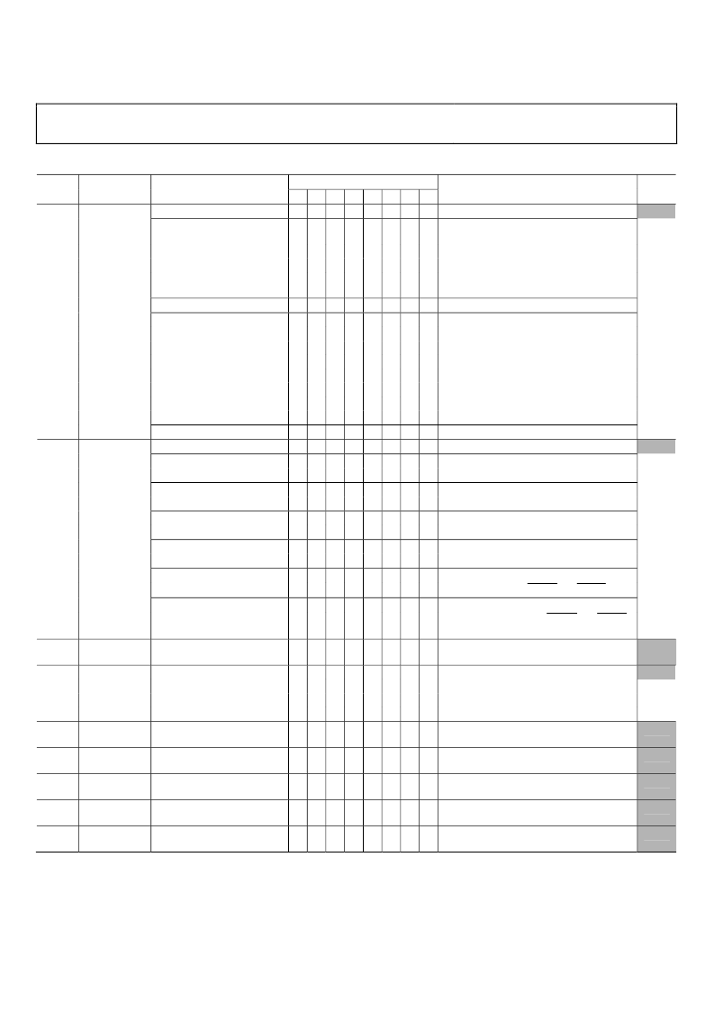
Table 14. Register 0x01 to Register 0x09
SR7 to
SR0
Register
0x01
Mode Select
Register
Rev. 0 | Page 26 of 96
Bit Description
Reserved.
DDR Clock Edge Alignment.
Note: Only used for ED
1
and
HD DDR modes.
Bit Number
5
4
Register Setting
Chroma clocked in on rising clock edge and
luma clocked in on falling clock edge.
Reserved.
Reserved.
Luma clocked in on rising clock edge and
chroma clocked in on falling clock edge.
SD input.
ED/HD-SDR input
2
ED/HD-DDR input.
Reserved.
Reserved.
Reserved.
Reserved.
ED (at 54 MHz) input.
Zero must be written to these bits.
Disabled.
Enabled.
Disable manual RGB matrix adjust.
Enable manual RGB matrix adjust.
No sync.
Sync on all RGB outputs.
RGB component outputs.
YPrPb component outputs.
No sync output.
Output SD syncs on HSYNC and VSYNC pins.
No sync output.
Output ED/HD syncs on HSYNC and VSYNC
pins.
LSBs for GY.
Reset
Value
0x00
7
6
3
2
0
1
0
0
0
0
1
1
1
0
1
Reserved.
Input Mode.
Note: See Reg. 0x30, Bits[7:3]
for ED/HD format selection.
0
0
1
0
0
0
0
1
1
1
1
0
1
0
0
1
1
0
0
1
1
0
1
0
1
0
1
0
1
0
1
0
1
0
0
1
0
1
0
0
Reserved.
Reserved.
Test Pattern Black Bar.
3
0x20
Manual RGB Matrix Adjust.
Sync on RGB.
RGB/YPrPb Output Select.
SD Sync Output Enable.
0x02
Mode
Register 0
ED/HD Sync Output Enable.
0x03
ED/HD CSC
Matrix 0
ED/HD CSC
Matrix 1
x
x
0x03
x
x
x
x
x
x
x
x
x
x
x
x
x
x
x
x
LSBs for RV.
LSBs for BU.
LSBs for GV.
LSBs for GU.
Bits[9:2] for GY.
0xF0
0x04
0x05
ED/HD CSC
Matrix 2
ED/HD CSC
Matrix 3
ED/HD CSC
Matrix 4
ED/HD CSC
Matrix 5
ED/HD CSC
Matrix 6
0x4E
0x06
x
x
x
x
x
x
x
x
Bits[9:2] for GU.
0x0E
0x07
x
x
x
x
x
x
x
x
Bits[9:2] for GV.
0x24
0x08
x
x
x
x
x
x
x
x
Bits[9:2] for BU.
0x92
0x09
x
x
x
x
x
x
x
x
Bits[9:2] for RV.
0x7C
1
ED = enhanced definition = 525p and 625p.
2
Available on the ADV7392/ADV7393 (40-pin devices) only.
3
Subaddress 0x31, Bit 2 must also be enabled (ED/HD). Subaddress 0x84, Bit 6 must also be enabled (SD).
相關(guān)PDF資料 |
PDF描述 |
|---|---|
| ADV7391EBZ | Low Power, Chip Scale 10-Bit SD/HD Video Encoder |
| ADV7392 | Low Power, Chip Scale 10-Bit SD/HD Video Encoder |
| ADV7392BCPZ | Low Power, Chip Scale 10-Bit SD/HD Video Encoder |
| ADV7392BCPZ-REEL | Low Power, Chip Scale 10-Bit SD/HD Video Encoder |
| ADV7392EBZ | Low Power, Chip Scale 10-Bit SD/HD Video Encoder |
相關(guān)代理商/技術(shù)參數(shù) |
參數(shù)描述 |
|---|---|
| ADV7391EBZ | 制造商:AD 制造商全稱:Analog Devices 功能描述:Low Power, Chip Scale 10-Bit SD/HD Video Encoder |
| ADV7391WBCPZ | 制造商:Analog Devices 功能描述: |
| ADV7391WBCPZ-RL | 制造商:Analog Devices 功能描述: |
| ADV7392 | 制造商:AD 制造商全稱:Analog Devices 功能描述:Low Power, Chip Scale 10-Bit SD/HD Video Encoder |
| ADV7392BCPZ | 制造商:Analog Devices 功能描述: |
發(fā)布緊急采購,3分鐘左右您將得到回復(fù)。