- 您現在的位置:買賣IC網 > PDF目錄374048 > ADV7391BCPZ-REEL (ANALOG DEVICES INC) Low Power, Chip Scale 10-Bit SD/HD Video Encoder PDF資料下載
參數資料
| 型號: | ADV7391BCPZ-REEL |
| 廠商: | ANALOG DEVICES INC |
| 元件分類: | 顏色信號轉換 |
| 英文描述: | Low Power, Chip Scale 10-Bit SD/HD Video Encoder |
| 中文描述: | COLOR SIGNAL ENCODER, QCC32 |
| 封裝: | 5 X 5 MM, ROHS COMPLIANT, MO-220VHHD-2, LFSCP-32 |
| 文件頁數: | 41/96頁 |
| 文件大小: | 1209K |
| 代理商: | ADV7391BCPZ-REEL |
第1頁第2頁第3頁第4頁第5頁第6頁第7頁第8頁第9頁第10頁第11頁第12頁第13頁第14頁第15頁第16頁第17頁第18頁第19頁第20頁第21頁第22頁第23頁第24頁第25頁第26頁第27頁第28頁第29頁第30頁第31頁第32頁第33頁第34頁第35頁第36頁第37頁第38頁第39頁第40頁當前第41頁第42頁第43頁第44頁第45頁第46頁第47頁第48頁第49頁第50頁第51頁第52頁第53頁第54頁第55頁第56頁第57頁第58頁第59頁第60頁第61頁第62頁第63頁第64頁第65頁第66頁第67頁第68頁第69頁第70頁第71頁第72頁第73頁第74頁第75頁第76頁第77頁第78頁第79頁第80頁第81頁第82頁第83頁第84頁第85頁第86頁第87頁第88頁第89頁第90頁第91頁第92頁第93頁第94頁第95頁第96頁
ADV7390/ADV7391/ADV7392/ADV7393
ADV7390/ADV7391 INPUT CONFIGURATION
The ADV7390/ADV7391 supports a number of different input
modes. The desired input mode is selected using Subaddress 0x01,
Bits[6:4]. The ADV7390/ADV7391 defaults to standard
definition (SD) mode upon power-up. Table 30 provides an
overview of all possible input configurations. Each input mode
is described in detail in this section.
Rev. 0 | Page 41 of 96
Table 30. ADV7390/ADV7391 Input Configuration
Input Mode
P7
000
SD
010
ED/HD-DDR
111
ED (at 54 MHz)
STANDARD DEFINITION
Subaddress 0x01, Bits[6:4] = 000
SD YCrCb data can be input in an interleaved 4:2:2 format over
an 8-bit bus rate of 27 MHz.
A 27 MHz clock signal must be provided on the CLKIN pin. If
required, external synchronization signals can be provided on
the HSYNC and VSYNC pins. Embedded EAV/SAV timing
codes are also supported. The ITU-R BT.601/656 input standard
is supported.
The interleaved pixel data is input on Pin P7 to Pin P0, with P0
being the LSB.
P6
P5
P4
YCrCb
YCrCb
YCrCb
P2
P2
P1
P0
MPEG2
DECODER
CLKIN
P[7:0]
27MHz
YCrCb
ADV7390/
ADV7391
VSYNC,
HSYNC
2
8
0
Figure 49. SD Example Application
ENHANCED DEFINITION/HIGH DEFINITION
Subaddress 0x01, Bits[6:4] = 010
ED or HD YCrCb data can be input in an interleaved 4:2:2
format over an 8-bit DDR bus.
The clock signal must be provided on the CLKIN pin. If
required, external synchronization signals can be provided on
the HSYNC and VSYNC pins. Embedded EAV/SAV timing
codes are also supported.
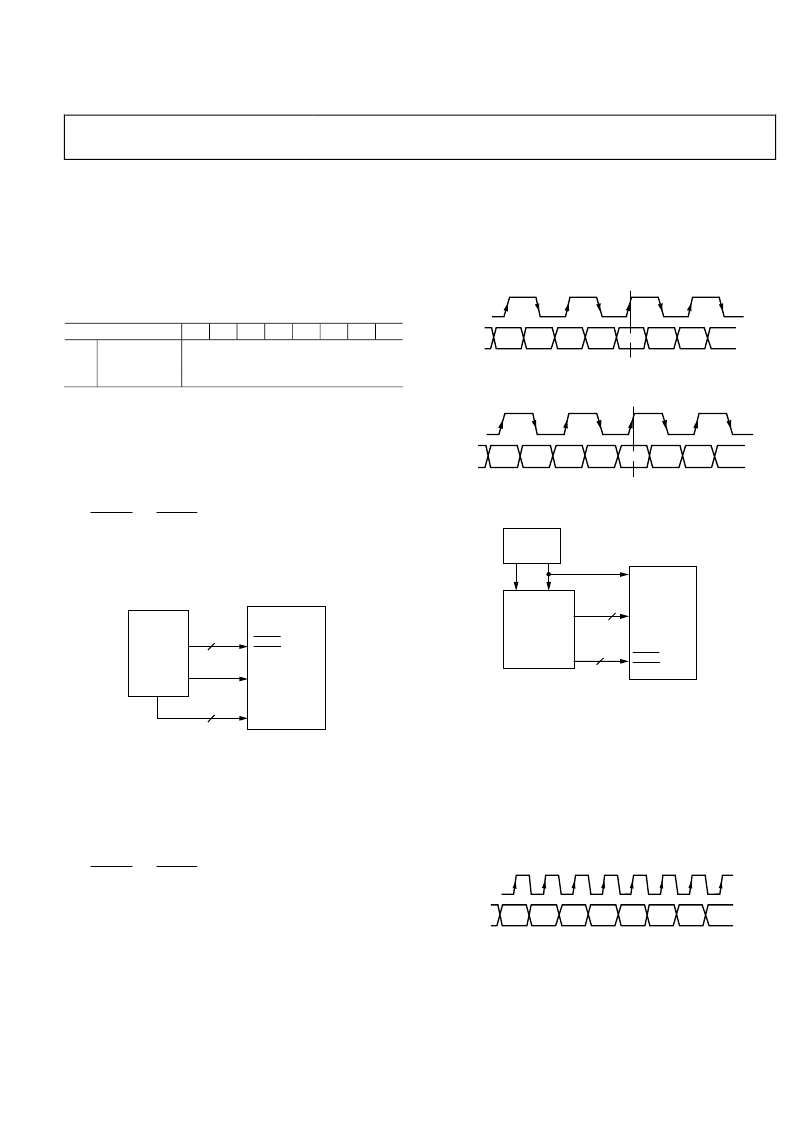
8-Bit 4:2:2 ED/HD YCrCb Mode (DDR)
In 8-bit DDR 4:2:2 YCrCb input mode, the Y pixel data is input
on Pin P7 to Pin P0 upon either the rising or falling edge of
CLKIN. P0 is the LSB.
The CrCb pixel data is also input on Pin P7 to Pin P0
upon the opposite edge of CLKIN. P0 is the LSB.
Whether the Y data is clocked in upon the rising or falling edge
of CLKIN is determined by Subaddress 0x01, Bits[2:1] (see
Figure 50 and Figure 51).
3FF
00
00
XY
Y0
Y1
Cr0
CLKIN
NOTES
1. SUBADDRESS 0x01 [2:1] SHOULD BE SET TO 00 IN THIS CASE.
Figure 50. ED/HD-DDR Input Sequence (EAV/SAV)—Option A
P[7:0]
Cb0
0
3FF
00
00
XY
Cb0
Cr0
Y1
CLKIN
P[7:0]
Y0
NOTES
1. SUBADDRESS 0x01 [2:1] SHOULD BE SET TO 11 IN THIS CASE.
0
Figure 51. ED/HD-DDR Input Sequence (EAV/SAV)—Option B
MPEG2
DECODER
CLKIN
P[7:0]
INTERLACED TO
PROGRESSIVE
YCrCb
ADV7390/
ADV7391
VSYNC,
HSYNC
8
2
YCrCb
0
Figure 52. ED/HD-DDR Example Application
ENHANCED DEFINITION (AT 54 MHz)
Subaddress 0x01, Bits[6:4] = 111
ED YCrCb data can be input in an interleaved 4:2:2 format over
an 8-bit bus rate of 54 MHz.
A 54 MHz clock signal must be provided on the CLKIN pin.
Embedded EAV/SAV timing codes are supported. External
synchronization signals are not supported in this mode.
The interleaved pixel data is input on Pin P7 to Pin P0, with P0
being the LSB.
3FF
00
00
XY
Cb0
Y0
Y1
Cr0
CLKIN
P[7:0]
0
Figure 53. ED (At 54 MHz) Input Sequence (EAV/SAV)
相關PDF資料 |
PDF描述 |
|---|---|
| ADV7391EBZ | Low Power, Chip Scale 10-Bit SD/HD Video Encoder |
| ADV7392 | Low Power, Chip Scale 10-Bit SD/HD Video Encoder |
| ADV7392BCPZ | Low Power, Chip Scale 10-Bit SD/HD Video Encoder |
| ADV7392BCPZ-REEL | Low Power, Chip Scale 10-Bit SD/HD Video Encoder |
| ADV7392EBZ | Low Power, Chip Scale 10-Bit SD/HD Video Encoder |
相關代理商/技術參數 |
參數描述 |
|---|---|
| ADV7391EBZ | 制造商:AD 制造商全稱:Analog Devices 功能描述:Low Power, Chip Scale 10-Bit SD/HD Video Encoder |
| ADV7391WBCPZ | 制造商:Analog Devices 功能描述: |
| ADV7391WBCPZ-RL | 制造商:Analog Devices 功能描述: |
| ADV7392 | 制造商:AD 制造商全稱:Analog Devices 功能描述:Low Power, Chip Scale 10-Bit SD/HD Video Encoder |
| ADV7392BCPZ | 制造商:Analog Devices 功能描述: |
發布緊急采購,3分鐘左右您將得到回復。