- 您現在的位置:買賣IC網 > PDF目錄374048 > ADVFC32SH (ANALOG DEVICES INC) Voltage-to-Frequency and Frequency-to-Voltage Converter PDF資料下載
參數資料
| 型號: | ADVFC32SH |
| 廠商: | ANALOG DEVICES INC |
| 元件分類: | 模擬專用變換器 |
| 英文描述: | Voltage-to-Frequency and Frequency-to-Voltage Converter |
| 中文描述: | VOLTAGE-FREQUENCY CONVERTER, 0.5 MHz, MBCY10 |
| 封裝: | TO-100, 10 PIN |
| 文件頁數: | 5/6頁 |
| 文件大小: | 141K |
| 代理商: | ADVFC32SH |
ADVFC32
REV. A
–5–
100 ppm/
°
C capacitor may result in a maximum overall circuit
gain drift of:
100 ppm/
°
C (ADVFC32BH) + 100 ppm/
°
C (C1)
+ 10 ppm/
°
C (R
IN
) = 210 ppm/
°
C
Although R
IN
and C1 have the most pronounced effect on tem-
perature stability, the offset circuit of resistors R4 and R5 may
also have a slight effect on the offset temperature drift of the cir-
cuit. T he offset will change with variations in the resistance of
R4 and supply voltage changes. In most applications the offset
adjustment is very small, and the offset drift attributable to this
circuit will be negligible. In the bipolar mode, however, both the
positive reference and the resistor used to offset the signal range
will have a pronounced effect on offset drift. A high quality
reference and resistor should be used to minimize offset drift
errors.
Other circuit components do not directly influence temperature
performance as long as their actual values are not so different
from nominal value as to preclude operation. T his includes
integration capacitor C2. A change in the capacitance value of
C2 results in a different rate of voltage change across C2, but
this is compensated by an equal effect when C2 is discharged by
the switched 1 mA current source so that no net effect occurs.
T he temperature effects of the components described above are
the same when the ADVFC32 is configured for negative or bi-
polar input ranges, or F/V conversion.
OT HE R CIRCUIT CONSIDE RAT IONS
T he input amplifier connected to Pins 1, 13, and 14 is not a
standard operational amplifier. Although it operates like an op
amp in most applications, two key differences should be noted.
First, the bias current of the positive input is typically 40 nA
while the bias current of the inverting input is
±
8 nA. T herefore,
any attempt to cancel input offset voltage due to bias currents by
matching input resistors will create worse offsets. Second, the
output of this amplifier will sink only 1 mA, even though it will
source as much as 10 mA. When used in the F/V mode, the am-
plifier must be buffered if large sink currents are required.
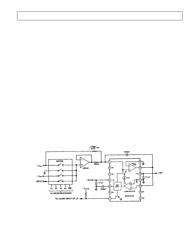
MICROPROCE SSOR OPE RAT E D A/D CONVE RT E R
With the addition of a few external components the ADVFC32
can be used as a
±
10 V A/D microprocessor front end. Although
the nonlinearity of the ADVFC32 is only 0.05% maximum
(0.01% typ), the resolution is much higher, allowing it to be
used in 16-bit measurement and control systems where a mono-
tonic transfer function is essential. T he resolution of the circuit
shown in Figure 5 is dependent on the amount of time allowed
to count the ADVFC32 frequency output. Using a full scale fre-
quency of 100 kHz, an 8-bit conversion can be made in about
10 ms, and a 2 second time period allows a 16-bit measurement,
including offset and gain calibration cycles.
As shown in Figure 5, the input signal is selected via the AD7590
input multiplexer. Positive and negative references as well as a
ground input are provided to calibrate the A/D. T his is very im-
portant in systems subject to moderate or extreme temperature
changes since the gain temperature coefficient of the ADVFC32
is as high as
±
150 ppm/
°
C. By using the calibration cycles, the
A/D conversion will be as accurate as the references provided.
T he AD542 following the input multiplexer provides a high im-
pedance input (10
12
ohms) and buffers the switch resistance
from the relatively low impedance ADVFC32 input.
If higher linearity is required, the ADVFC32 can be operated at
10 kHz, but this will require a proportionately longer conver-
sion, time. Conversely, the conversion time can be decreased at
the expense of nonlinearity by increasing the maximum fre-
quency to as high as 500 kHz.
HIGH NOISE IMMUNIT Y , HIGH CMRR ANALOG DAT A
LINK
In many applications, a signal must be sensed at a remote site
and sent through a very noisy environment to a central location
for further processing. In these cases, even a shielded cable may
not protect the signal from noise pickup. T he circuit of Figure 6
provides a solution in these cases. Due to the optocoupler and
Figure 5. High Resolution, Self-Calibrating, Microprocessor
Operated A/D Converter
voltage-to-frequency conversion, this data link is extremely
insensitive to noise and common-mode voltage interference. For
even more protection, an optical fiber link substituted for the
HCPL2630 will provide common-mode rejection of more than
several hundred kilovolts and virtually total immunity to electri-
cal noise. For most applications, however, the frequency modu-
lated
signal has sufficient noise immunity without using an optical
相關PDF資料 |
PDF描述 |
|---|---|
| ADXL105EM-1 | ADXL105/ADXL150/ADXL250/ADXL190 Evaluation Modules |
| ADXL105EM-3 | ADXL105/ADXL150/ADXL250/ADXL190 Evaluation Modules |
| ADXL150EM-1 | ADXL105/ADXL150/ADXL250/ADXL190 Evaluation Modules |
| ADXL150EM-3 | ADXL105/ADXL150/ADXL250/ADXL190 Evaluation Modules |
| ADXL190EM-1 | ADXL105/ADXL150/ADXL250/ADXL190 Evaluation Modules |
相關代理商/技術參數 |
參數描述 |
|---|---|
| ADVFC32SH/883B | 功能描述:電壓頻率轉換及頻率電壓轉換 IC MONO V/F AND F/V CONV RoHS:否 制造商:Texas Instruments 全標度頻率:4000 KHz 線性誤差:+/- 1 % FSR 電源電壓-最大: 電源電壓-最小: 最大工作溫度:+ 85 C 最小工作溫度:- 25 C 安裝風格:Through Hole 封裝 / 箱體:PDIP-14 封裝:Tube |
| ADVFEEDTHRU001 | 制造商:AVX Corporation 功能描述:DESIGN KIT FEEDTHROUGH CAPACITORS 制造商:AVX Corporation 功能描述:DESIGN KIT, FEEDTHROUGH CAPACITORS 制造商:AVX Corporation 功能描述:DESIGN KIT, FEEDTHROUGH CAPACITORS; Kit Contents:26 Feedthrough Capacitors ;RoHS Compliant: Yes |
| A-DVI-1001-01-R | 制造商:Assmann Electronics Inc 功能描述:CONN DVI-D MALE SLDR |
| A-DVI-1001-02-R | 制造商:Assmann Electronics Inc 功能描述:CONN DVI MALE SLDR |
| A-DVI-1002-01-R | 制造商:Assmann Electronics Inc 功能描述:CONN DVI MALE SLDR |
發(fā)布緊急采購,3分鐘左右您將得到回復。