- 您現(xiàn)在的位置:買賣IC網(wǎng) > PDF目錄379669 > AN231K04-DVLP3 (Electronic Theatre Controls, Inc.) Dynamically Reconfigurable dpASP PDF資料下載
參數(shù)資料
| 型號: | AN231K04-DVLP3 |
| 廠商: | Electronic Theatre Controls, Inc. |
| 英文描述: | Dynamically Reconfigurable dpASP |
| 中文描述: | 動態(tài)可重構(gòu)dpASP |
| 文件頁數(shù): | 7/24頁 |
| 文件大小: | 445K |
| 代理商: | AN231K04-DVLP3 |
AN231E04 Datasheet – Dynamically Reconfigurable dpASP
DS231000-U001d
- 7 -
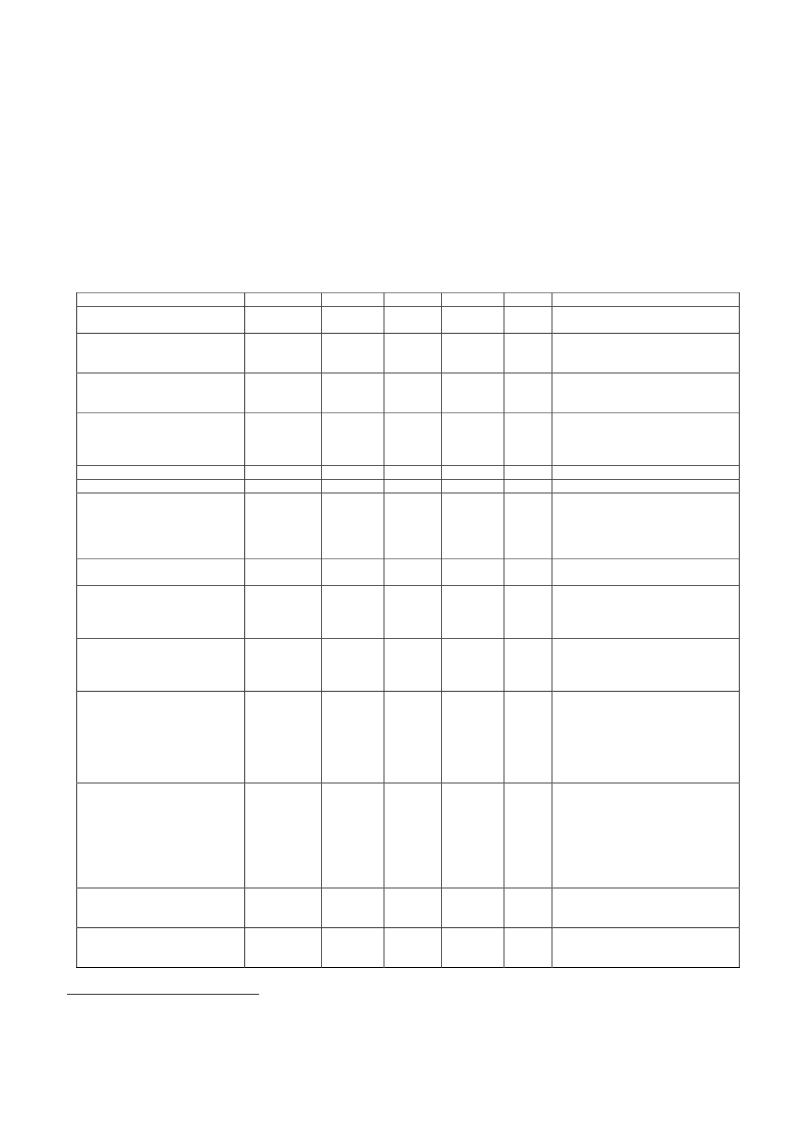
1.4 Digital I/O Characteristics continued (VDD = 3.3v +/-10%, -40 to 85 deg.C unless commented)
1.4.6
Pin LCCb/DOUT1 (CMOS Output)
The primary function of this pin is as LCCb (Local Configuration Complete), this signal is used in multiple dpASP designs to
pass Chips Select from dpASP to dpASP enabling primary configuration of a serial chain of dpASP’s from a single SPI bus,
please refer to the AN231E04 User Guide for details.
If the LCCb signal pin is not required (e.g. a circuit design with a single dpASP device) then via dpASP configuration this pin
can be used as a digital output, this is realized by adjusting the properties of the dpASP “digital I/O cell”.
Parameter
Symbol
Min
Typ
Max
Unit
Comment
Load 10pF//50Kohm to VSS,
during configuration.
Load 10pF//50Kohm to VSS,
during configuration.
VDD = 3.3 V
Load 10pF//50Kohm to VSS,
When configured to
pin39=DOUT1
Load 10pF//50Kohm to VSS,
When configured to
pin39=DOUT1
VDD = 3.3 V.
Maximum load 10 pF // 50 Kohm
Maximum load 10 pF // 50 Kohm
LCCb (pin 39) shorted to VDD,
during configuration.
Current should be limited
externally so that it does not
exceed 3mA.
LCCb (pin 39) shorted to VSS,
during configuration.
DOUT1 (pin 39) shorted to VDD,.
Current should be limited
externally so that it does not
exceed 3mA.
DOUT1 (pin 39) shorted to VSS,
Current should be limited
externally so that it does not
exceed 3mA.
Skew at DOUT1 (pin 39) relative to
external signal clock applied to
input pin ACLK (pin 34).
Note; This is only valid when
DOUT1 is selected to output the
CAM clockA, and CAM clockA is
derived from ACLK divided by1.
This is the delay of the comparator
CAM output transition relative to
the exported comparator clock
clock appears on the output pin.
Note, The comparator is clocked
with a user programmable CAM
clock derived from a division of
ACLK
This is the delay of the signal at the
dpASP pin 39, (DOUT1) relative to
the actual internal transfer event.
This is the delay of the signal at the
dpASP pin 39, (DOUT1) relative to
the actual internal event.
Output Voltage Low, (LCCb)
Vol(LCCb)
VSS
-
VSS
mV
Output Voltage High, (LCCb)
Voh(LCCb)
3.00
-
3.20
V
Output Voltage Low, (DOUT1)
Vol(DOUT1)
VSS
-
VSS
mV
Output Voltage High, (DOUT1)
Voh(DOUT1)
3.29
-
VDD
V
Max. Capacitive Load
Min. Resistive Load
Cmax
Rmin
-
-
-
10
-
pF
Kohm
50
Current Sink, (LCCb)
Isnk(LCCb)
3.0
-
7.0
mA
Current Source, (LCCb)
Isrc(LCCb)
0.25
-
0.80
mA
Current Sink, (DOUT1)
Isnk(DOUT1)
20.0
-
60.0
mA
Current Source, (DOUT1)
Isrc(DOUT1)
12.5
-
35.0
mA
Clock skew
(DOUT1 connected to
“clocka”)
CLK
SKEW
-
8.0
-
ns
Comparator skew
(DOUT1 connected to
“comparator”)
COMP
SKEW
-
25.0
-
ns
RAM transfer delay
(DOUT1 connected to “RAM
transfer Pulse”)
Auto-null/Osc start delay
(DOUT1 connected to “Auto-
null/Osc start done” signal)
1
RAM
DELAY
-
20.0
-
ns
DONE
DELAY
-
40
-
ms
1
see application note AN231002 “Auto-nulling within the AN231E04”
相關(guān)PDF資料 |
PDF描述 |
|---|---|
| AN321 | AND / NOR circuit providing the logical function |
| AN3791 | VTR X-VALUE SHIFT CIRCUIT |
| AN53 | The CS5322 Digital Filter |
| AN7203 | FM FRONT-END IC FOR RADIO, RADIO CASSETTE RECORDER |
| AN80T05LF | AN80T05LF (IC901) : REGULATOR |
相關(guān)代理商/技術(shù)參數(shù) |
參數(shù)描述 |
|---|---|
| AN232 | 制造商:MICROCHIP 制造商全稱:Microchip Technology 功能描述:Low Frequency Magnetic Transmitter Design |
| AN2320S | 制造商:未知廠家 制造商全稱:未知廠家 功能描述:Video Camera Circuit |
| AN23-23A | 制造商:AN# - MILITARY 功能描述: |
| AN23-25A | 制造商:AN# - MILITARY 功能描述: |
| AN232ISO | 制造商:未知廠家 制造商全稱:未知廠家 功能描述:simple and effective protection against all surges, static electricity and ground loops in your RS232 line. |
發(fā)布緊急采購,3分鐘左右您將得到回復(fù)。