- 您現在的位置:買賣IC網 > PDF目錄379698 > ATT3042-70H84I (Electronic Theatre Controls, Inc.) Field-Programmable Gate Arrays PDF資料下載
參數資料
| 型號: | ATT3042-70H84I |
| 廠商: | Electronic Theatre Controls, Inc. |
| 元件分類: | FPGA |
| 英文描述: | Field-Programmable Gate Arrays |
| 中文描述: | 現場可編程門陣列 |
| 文件頁數: | 35/80頁 |
| 文件大小: | 528K |
| 代理商: | ATT3042-70H84I |
第1頁第2頁第3頁第4頁第5頁第6頁第7頁第8頁第9頁第10頁第11頁第12頁第13頁第14頁第15頁第16頁第17頁第18頁第19頁第20頁第21頁第22頁第23頁第24頁第25頁第26頁第27頁第28頁第29頁第30頁第31頁第32頁第33頁第34頁當前第35頁第36頁第37頁第38頁第39頁第40頁第41頁第42頁第43頁第44頁第45頁第46頁第47頁第48頁第49頁第50頁第51頁第52頁第53頁第54頁第55頁第56頁第57頁第58頁第59頁第60頁第61頁第62頁第63頁第64頁第65頁第66頁第67頁第68頁第69頁第70頁第71頁第72頁第73頁第74頁第75頁第76頁第77頁第78頁第79頁第80頁
Data Sheet
February 1997
ATT3000 Series Field-Programmable Gate Arrays
Lucent Technologies Inc.
35
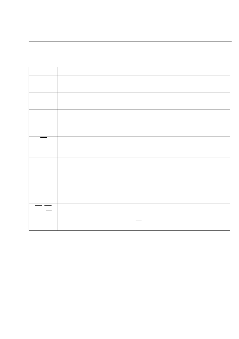
Pin Information
(continued)
Table 5. I/O Pins with Special Functions
Symbol
Name/Description
M2
Mode 2
. This input has a passive pull-up during configuration. Together with M0 and M1, it is
sampled before the start of configuration to establish the configuration mode to be used. After
configuration, this pin becomes a user-programmable I/O pin.
HDC
High During Configuration
. HDC is held at a high level by the FPGA until after configuration. It
is available as a control output indicating that configuration is not yet completed. After
configuration, this pin is a user I/O pin.
LDC
Low During Configuration
. This active-low signal is held at a low level by the FPGA until after
configuration. It is available as a control output indicating that configuration is not yet completed.
It is particularly useful in master mode as a low enable for an EPROM. After configuration, this
pin is a user I/O pin. If used as a low EPROM enable, it must be programmed as a high after
configuration.
INIT
This is an active-low, open-drain output which is held low during the power stabilization and
internal clearing of the configuration memory. It can be used to indicate status to a configuring
microprocessor or, as a wired-AND of several slave mode devices, a hold-off signal for a master
mode device. After configuration, this pin becomes a user-programmable I/O pin.
BCLKIN
This is a direct CMOS level input to the alternate clock buffer (auxiliary buffer) in the lower right
corner.
XTL1
This user I/O pin can be used to operate as the output of an amplifier driving an external crystal
and bias circuitry.
XTL2
This user I/O pin can be used as the input of an amplifier connected to an external crystal and
bias circuitry. The I/O block is left unconfigured. The oscillator configuration is activated by
routing a net from the oscillator buffer symbol output and by the
ORCA
Foundry bit stream
generation program.
CS0
,
CS1
,
CS2,
WS
These four inputs represent a set of signals, three active-low and one active-high, which are
used in the peripheral mode to control configuration data entry. The assertion of all four
generates a write to the internal data buffer. The removal of any assertion clocks in the D[7:0]
data present. In the master parallel mode,
WS
and CS2 are the A0 and A1 outputs. After
configuration, the pins are user-programmable I/O pins.
相關PDF資料 |
PDF描述 |
|---|---|
| ATT3042-70J132I | Field-Programmable Gate Arrays |
| ATT3042-70J44I | Field-Programmable Gate Arrays |
| ATT3042-70J68I | Field-Programmable Gate Arrays |
| ATT3042-70J84I | Field-Programmable Gate Arrays |
| ATT3042-70M132I | Field-Programmable Gate Arrays |
相關代理商/技術參數 |
參數描述 |
|---|---|
| ATT3042-70J100 | 制造商:未知廠家 制造商全稱:未知廠家 功能描述:Field Programmable Gate Array (FPGA) |
| ATT3042-70J100I | 制造商:未知廠家 制造商全稱:未知廠家 功能描述:Field Programmable Gate Array (FPGA) |
| ATT3042-70J132I | 制造商:未知廠家 制造商全稱:未知廠家 功能描述:Field-Programmable Gate Arrays |
| ATT3042-70J44I | 制造商:未知廠家 制造商全稱:未知廠家 功能描述:Field-Programmable Gate Arrays |
| ATT3042-70J68I | 制造商:未知廠家 制造商全稱:未知廠家 功能描述:Field-Programmable Gate Arrays |
發布緊急采購,3分鐘左右您將得到回復。