- 您現在的位置:買賣IC網 > PDF目錄379698 > ATT3042-70H84I (Electronic Theatre Controls, Inc.) Field-Programmable Gate Arrays PDF資料下載
參數資料
| 型號: | ATT3042-70H84I |
| 廠商: | Electronic Theatre Controls, Inc. |
| 元件分類: | FPGA |
| 英文描述: | Field-Programmable Gate Arrays |
| 中文描述: | 現場可編程門陣列 |
| 文件頁數: | 5/80頁 |
| 文件大小: | 528K |
| 代理商: | ATT3042-70H84I |
第1頁第2頁第3頁第4頁當前第5頁第6頁第7頁第8頁第9頁第10頁第11頁第12頁第13頁第14頁第15頁第16頁第17頁第18頁第19頁第20頁第21頁第22頁第23頁第24頁第25頁第26頁第27頁第28頁第29頁第30頁第31頁第32頁第33頁第34頁第35頁第36頁第37頁第38頁第39頁第40頁第41頁第42頁第43頁第44頁第45頁第46頁第47頁第48頁第49頁第50頁第51頁第52頁第53頁第54頁第55頁第56頁第57頁第58頁第59頁第60頁第61頁第62頁第63頁第64頁第65頁第66頁第67頁第68頁第69頁第70頁第71頁第72頁第73頁第74頁第75頁第76頁第77頁第78頁第79頁第80頁
Data Sheet
February 1997
ATT3000 Series Field-Programmable Gate Arrays
Lucent Technologies Inc.
5
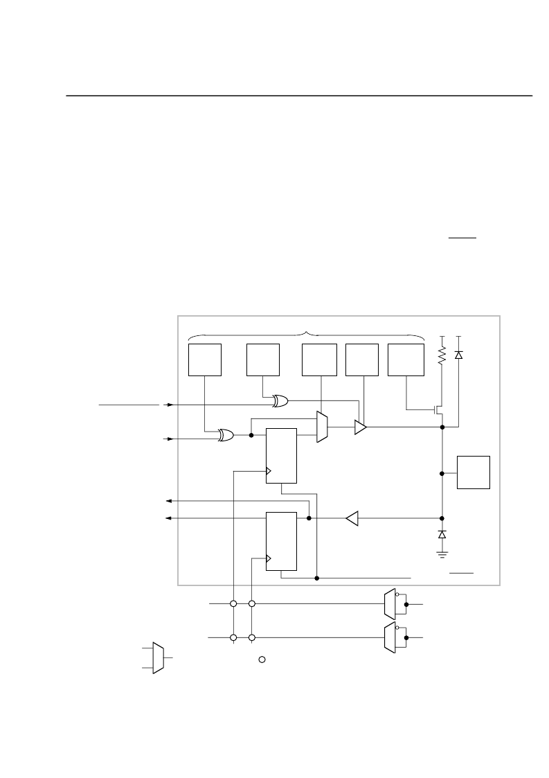
I/O Block
Each user-configurable I/O block (IOB), shown in
Figure 3, provides an interface between the external
package pin of the device and the internal user logic.
Each IOB includes both registered and direct input
paths and a programmable 3-state output buffer which
may be driven by a registered or direct output signal.
Configuration options allow each IOB an inversion, a
controlled slew rate, and a high-impedance pull-up.
Each input circuit also provides input clamping diodes
to provide electrostatic protection and circuits to inhibit
latch-up produced by input currents.
The input buffer portion of each IOB provides threshold
detection to translate external signals applied to the
package pin to internal logic levels. The global input-
buffer threshold of the IOB can be programmed to be
compatible with either TTL or CMOS levels. The buff-
ered input signal drives the data input of a storage
element which may be configured as a positive-edge
triggered D flip-flop or a low-level transparent latch. The
sense of the clock can be inverted (negative edge/high
transparent) as long as all IOBs on the same clock net
use the same clock sense. Clock/load signals (IOB pins
.ik and .ok) can be selected from either of two die edge
metal lines. I/O storage elements are reset during con-
figuration or by the active-low chip
RESET
input. Both
direct input (from IOB pin .i) and registered input (from
IOB pin .q) signals are available for interconnect.
Figure 3. Input/Output Block
5-3102(F)
OUT
INVERT
3-STATE
INVERT
OUTPUT
SELECT
SLEW
RATE
PASSIVE
PULL UP
PROGRAM-CONTROLLED MEMORY CELLS
V
CC
OUTPUT
BUFFER
FLIP-
FLOP
D
Q
R
TTL OR
CMOS
INPUT
THRESHOLD
FLIP-
FLOP
OR
LATCH
Q
D
R
.lk
.t
= PROGRAMMABLE INTERCONNECTION POINT OR PIP
CK2
(GLOBAL RESET)
I/O PAD
.o
.i
.q
3-STATE
OUT
DIRECT IN
REGISTERED IN
CK1
PROGRAM-
CONTROLLED
MULTIPLEXER
OUTPUT ENABLE
.ok
相關PDF資料 |
PDF描述 |
|---|---|
| ATT3042-70J132I | Field-Programmable Gate Arrays |
| ATT3042-70J44I | Field-Programmable Gate Arrays |
| ATT3042-70J68I | Field-Programmable Gate Arrays |
| ATT3042-70J84I | Field-Programmable Gate Arrays |
| ATT3042-70M132I | Field-Programmable Gate Arrays |
相關代理商/技術參數 |
參數描述 |
|---|---|
| ATT3042-70J100 | 制造商:未知廠家 制造商全稱:未知廠家 功能描述:Field Programmable Gate Array (FPGA) |
| ATT3042-70J100I | 制造商:未知廠家 制造商全稱:未知廠家 功能描述:Field Programmable Gate Array (FPGA) |
| ATT3042-70J132I | 制造商:未知廠家 制造商全稱:未知廠家 功能描述:Field-Programmable Gate Arrays |
| ATT3042-70J44I | 制造商:未知廠家 制造商全稱:未知廠家 功能描述:Field-Programmable Gate Arrays |
| ATT3042-70J68I | 制造商:未知廠家 制造商全稱:未知廠家 功能描述:Field-Programmable Gate Arrays |
發(fā)布緊急采購,3分鐘左右您將得到回復。