- 您現(xiàn)在的位置:買賣IC網(wǎng) > PDF目錄19023 > DC1370A-J (Linear Technology)BOARD DEMO 65MSPS LTC2258-12 PDF資料下載
參數(shù)資料
| 型號(hào): | DC1370A-J |
| 廠商: | Linear Technology |
| 文件頁數(shù): | 16/34頁 |
| 文件大小: | 0K |
| 描述: | BOARD DEMO 65MSPS LTC2258-12 |
| 軟件下載: | QuikEval II System |
| 設(shè)計(jì)資源: | DC1370A Design Files |
| 標(biāo)準(zhǔn)包裝: | 1 |
| 系列: | * |
| 相關(guān)產(chǎn)品: | DC718C-ND - DEMO QUIKEVAL-II DATA |
第1頁第2頁第3頁第4頁第5頁第6頁第7頁第8頁第9頁第10頁第11頁第12頁第13頁第14頁第15頁當(dāng)前第16頁第17頁第18頁第19頁第20頁第21頁第22頁第23頁第24頁第25頁第26頁第27頁第28頁第29頁第30頁第31頁第32頁第33頁第34頁
LTC2258-12
LTC2257-12/LTC2256-12
23
225812fd
For more information www.linear.com/LTC2258-12
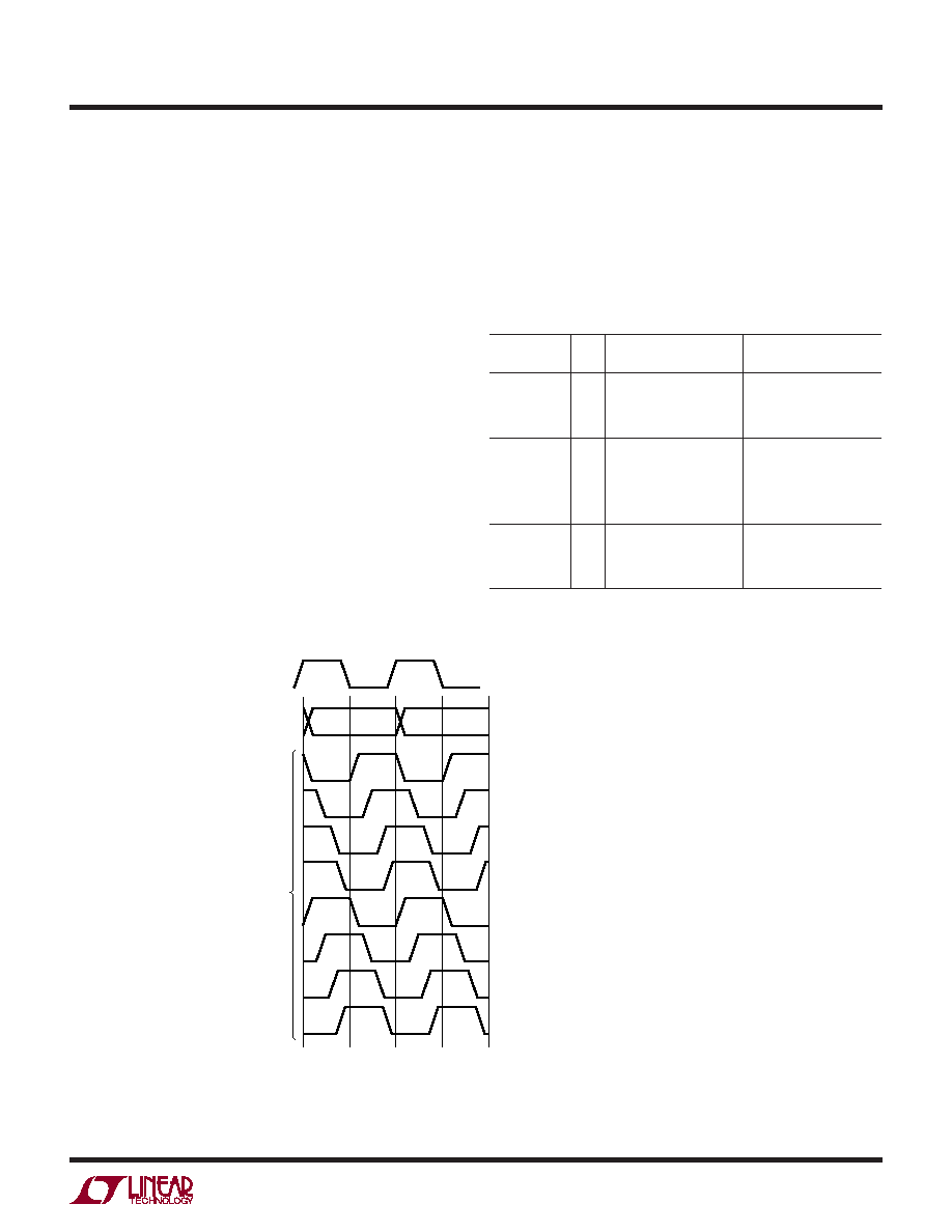
Phase Shifting the Output Clock
In full-rate CMOS mode the data output bits normally
change at the same time as the falling edge of CLKOUT+,
so the rising edge of CLKOUT+ can be used to latch the
output data. In double data rate CMOS and LVDS modes
the data output bits normally change at the same time as
the falling and rising edges of CLKOUT+. To allow adequate
setup-and-hold time when latching the data, the CLKOUT+
signal may need to be phase shifted relative to the data
output bits. Most FPGAs have this feature; this is generally
the best place to adjust the timing.
TheLTC2258-12/LTC2257-12/LTC2256-12canalsophase
shift the CLKOUT+/CLKOUT– signals by serially program-
ming mode control register A2. The output clock can be
shifted by 0°, 45°, 90° or 135°. To use the phase shifting
feature the clock duty cycle stabilizer must be turned
on. Another control register bit can invert the polarity of
CLKOUT+ and CLKOUT–, independently of the phase shift.
Thecombinationofthesetwofeaturesenablesphaseshifts
of 45° up to 315° (Figure 14).
DATA FORMAT
Table 1 shows the relationship between the analog input
voltage, the digital data output bits and the overflow bit.
By default the output data format is offset binary. The 2’s
complement format can be selected by serially program-
ming mode control register A4.
Table 1. Output Codes vs Input Voltage
AIN+ – AIN–
(2V RANGE)
OF
D11-D0
(OFFSET BINARY)
D11-D0
(2’s COMPLEMENT)
>+1.000000V
+0.999512V
+0.999024V
1
0
1111 1111 1111
1111 1111 1110
0111 1111 1111
0111 1111 1110
+0.000488V
0.000000V
–0.000488V
–0.000976V
0
1000 0000 0001
1000 0000 0000
0111 1111 1111
0111 1111 1110
0000 0000 0001
0000 0000 0000
1111 1111 1111
1111 1111 1110
–0.999512V
–1.000000V
≤–1.000000V
0
1
0000 0000 0001
0000 0000 0000
1000 0000 0001
1000 0000 0000
applicaTions inForMaTion
CLKOUT+
D0-D11, OF
PHASE
SHIFT
0°
45°
90°
135°
180°
225°
270°
315°
CLKINV
0
1
CLKPHASE1
MODE CONTROL BITS
0
1
0
1
CLKPHASE0
0
1
0
1
0
1
0
1
225812 F14
ENC+
Figure 14. Phase Shifting CLKOUT
相關(guān)PDF資料 |
PDF描述 |
|---|---|
| 17 | LAMP T1-3/4 WEDGE BASE |
| CL-830-R23-XT | CHROMALIT XT LIGHT SOURCE RND |
| 85- | T1-3/4 28V WEDGE BASE |
| 93 | LAMP INCAND S-8 S.C. BAYONET |
| A3CT-7011 | SWITCH UNIT-IP40 |
相關(guān)代理商/技術(shù)參數(shù) |
參數(shù)描述 |
|---|---|
| DC1370A-K | 功能描述:BOARD DEMO 40MSPS LTC2257-12 RoHS:是 類別:未定義的類別 >> 其它 系列:* 標(biāo)準(zhǔn)包裝:1 系列:* 其它名稱:MS305720A |
| DC1370A-L | 功能描述:BOARD DEMO 25MSPS LTC2256-12 RoHS:是 類別:未定義的類別 >> 其它 系列:* 標(biāo)準(zhǔn)包裝:1 系列:* 其它名稱:MS305720A |
| DC1370A-M | 制造商:Linear Technology 功能描述:14BIT ADC Eval Brd, Rq. DC718 制造商:Linear Technology 功能描述:14BIT ADC Eval Brd, Rq. DC718; Silicon Manufacturer:Linear Technology; Silicon Core Number:LTC2262-14; Kit Application Type:Data Converter; Application Sub Type:ADC; Kit Contents:Board, Guide; Features:Also works with requred DC718 |
| DC1370A-N | 制造商:Linear Technology 功能描述:12BIT ADC Eval Brd, Rq. DC718 制造商:Linear Technology 功能描述:12BIT ADC Eval Brd, Rq. DC718; Silicon Manufacturer:Linear Technology; Silicon Core Number:LTC2262-12; Kit Application Type:Data Converter; Application Sub Type:ADC; Kit Contents:Board, Guide; Features:Also works with requred DC718 |
| DC1371A | 功能描述:BOARD USB DATA ACQUISITION HS RoHS:是 類別:未定義的類別 >> 其它 系列:* 標(biāo)準(zhǔn)包裝:1 系列:* 其它名稱:MS305720A |
發(fā)布緊急采購,3分鐘左右您將得到回復(fù)。