- 您現(xiàn)在的位置:買賣IC網(wǎng) > PDF目錄376632 > DEM-VSP2232Y (Texas Instruments, Inc.) CCD SIGNAL PROCESSOR FOR DIGITAL CAMERAS PDF資料下載
參數(shù)資料
| 型號: | DEM-VSP2232Y |
| 廠商: | Texas Instruments, Inc. |
| 英文描述: | CCD SIGNAL PROCESSOR FOR DIGITAL CAMERAS |
| 中文描述: | CCD信號處理器的數(shù)碼相機(jī) |
| 文件頁數(shù): | 9/19頁 |
| 文件大小: | 248K |
| 代理商: | DEM-VSP2232Y |
VSP2232
SLAS320
–
MAY 2001
9
www.ti.com
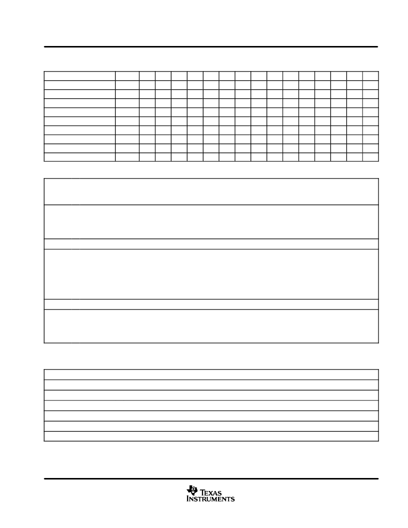
Table 2. Serial Interface Data Format
MSB
LSB
REGISTERS
TEST
A2
A1
A0
D11
D10
D9
D8
D7
D6
D5
D4
D3
D2
D1
D0
Configuration
0
0
0
0
0
0
0
C8
0
0
0
0
0
0
0
C0
PGA gain
0
0
0
1
0
0
G9
G8
G7
G6
G5
G4
G3
G2
G1
G0
OB clamp level
0
0
1
0
0
0
0
0
0
0
0
0
O3
O2
O1
O0
Clock polarity
0
0
1
1
0
0
0
0
0
0
0
0
0
P2
P1
P0
Output delay
0
1
0
0
0
0
0
0
0
0
0
0
0
0
J1
J0
Reserved
0
1
0
1
x
x
x
x
x
x
x
x
x
x
x
x
Reserved
0
1
1
0
x
x
x
x
x
x
x
x
x
x
x
x
Reserved
0
1
1
1
x
x
x
x
x
x
x
x
x
x
x
x
Reserved
x = Don
’
t care
1
x
x
x
x
x
x
x
x
x
x
x
x
x
x
x
C0
: Operation Mode, Normal/Standby
Serial interface and registers are always active, independently from the operation mode
C0 = 0 Normal operation,
C0 = 1 Standby
:
A/D Converter Drive Mode, Internal/External
Internal drive mode: The clock is internally generated by SHP and SHP drives the A/D converter
External drive mode: The master clock (ADCCK) drives the A/D converter
C8 = 0 Internal drive mode,
C8 = 1 External drive mode
:
Characteristics of PGA Gain (see Figure 2)
:
Additional Output Delay Control
Controls additional output data delay time
J1 = 0, J0 = 0
Additional Delay = 0 ns
J1 = 0, J0 = 1
Additional Delay = 5 ns (typ)
J1 = 1, J0 = 0
Additional Delay = 10 ns (typ)
J1 = 1, J0 = 1
Additional Delay = 13 ns (typ)
:
Programmable OB Clamp Level (see Table 1)
:
Clock Polarity
P0 = Polarity for CLPDM
(P0 = 0 active low, P0 = 1 active high)
P1 = for CLPOB
(P0 = 0 active low, P0 = 1 active high)
P2 = for SHP/SHD
(P0 = 0 active low, P0 = 1 active high)
C8
G[9:0]
J[1:0]
O[3:0]
P[2:0]
Right after power on, these values are unknown. They must be set to the appropriate value using the serial
interface, or reset to the default value by the RESET pin.
Default values are:
C0 = 0
C8 = 0
G[9:0] = 0010000000
J[1:0] = 00
O[3:0] = 1000
P[2:0] = 000
NOTE 6: The description and the timing diagrams in this data sheet are all based on the polarity of active low (default value).
:
:
:
:
:
:
Normal operation mode
A/D converter internal drive mode
PGA gain = 0 dB
Additional output delay = 0 ns
OB clamp level = 32 LSB
CLPDM, CLPOB, SHP/SHD are all active low (see Note 6)
相關(guān)PDF資料 |
PDF描述 |
|---|---|
| DEM16101H | LCD MODULE |
| DEM16101SYH | DEM16101SYH |
| DEM16216SYH-LY | DEM16216SYH-LY |
| DEM16216SYH-PY | Display Elektronik GmbH |
| DEM16217SYH | Display Elektronik GmbH |
相關(guān)代理商/技術(shù)參數(shù) |
參數(shù)描述 |
|---|---|
| DEM-VSP2260Y | 制造商:Rochester Electronics LLC 功能描述:- Bulk |
| DEM-VSP2262Y | 制造商:Texas Instruments 功能描述:EVAL BD FOR CCD SGNL PROCESSOR FOR DGTL CAMERAS - Bulk |
| DEM-VSP3100Y | 制造商:Texas Instruments 功能描述:EVALUATION/DEMO BOARD FOR VSP3100Y - Bulk |
| DEMX-5W1P-1AON-K87 | 制造商:ITT Interconnect Solutions 功能描述:DEMX-5W1P-1AON-K87 - Bulk |
| DEMX5W1PK87 | 制造商:ITT 功能描述:DSUB 5W1 M PCR/A G50 T 制造商:ITT Interconnect Solutions 功能描述:DSUB 5W1 M PCR/A G50 T |
發(fā)布緊急采購,3分鐘左右您將得到回復(fù)。