- 您現在的位置:買賣IC網 > PDF目錄376702 > DG188BA (HARRIS SEMICONDUCTOR) High-Speed Drivers with JFET Switch PDF資料下載
參數資料
| 型號: | DG188BA |
| 廠商: | HARRIS SEMICONDUCTOR |
| 元件分類: | 運動控制電子 |
| 英文描述: | High-Speed Drivers with JFET Switch |
| 中文描述: | 1-CHANNEL, SGL POLE DOUBLE THROW SWITCH, MBCY10 |
| 文件頁數: | 1/9頁 |
| 文件大小: | 75K |
| 代理商: | DG188BA |
CAUTION: These devices are sensitive to electrostatic discharge. Users should follow proper I.C. Handling Procedures.
Copyright
Harris Corporation 1999
1
Semiconductor
DG181 thru DG191
High-Speed Drivers with JFET Switch
Description
The DG181 thru DG191 series of analog gates consist of 2
or 4 N-channel junction-type field-effect transistors (JFET)
designed to function as electronic switches. Level-shifting
drivers enable low-level inputs (0.8V to 2V) to control the
ON-OFF state of each switch. The driver is designed to
provide a turn-off speed which is faster than turn-on speed,
so
that
break-before-make
switching from one channel to another. In the ON state, each
switch conducts current equally well in both directions. In the
OFF condition, the switches will block voltages up to 20V
peak-to-peak. Switch-OFF input-output isolation 50dB at
10MHz, due to the low output impedance of the FET-gate
driving circuit.
action
is
achieved
when
Features
Constant ON-Resistance for Signals to
±
10V (DG182,
DG185, DG188, DG191), to
±
7.5V (All Devices)
±
15V Power Supplies
<2nA Leakage from Signal Channel in Both ON and
OFF States
TTL, DTL, RTL Direct Drive Compatibility
t
ON
, t
OFF
<150ns, Break-Before-Make Action
Cross-Talk and Open Switch Isolation >50dB at 10MHz
(75
Load)
April 1999
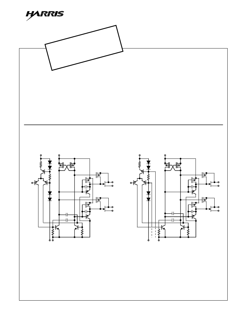
Functional Diagrams (Typical Channel)
DG186, DG187, DG188 - ONE AND TWO CHANNEL
SPDT AND SPST CIRCUIT CONFIGURATION
DG183, DG184, DG185 - TWO CHANNEL DPST
CIRCUIT CONFIGURATION
S
2
D
2
S
1
D
1
V+
GND
V
L
IN
V-
S
D
S
D
V+
GND
V
L
IN
V-
File Number
3114.4
POSOBSOLETE PRODUCT
DG184, DG185: HI-5049, HI-5045
相關PDF資料 |
PDF描述 |
|---|---|
| DG1H3_07 | Schottky Barrier Diode |
| DG1H3A | Schottky Barrier Diode |
| DG1J10A | Schottky Barrier Diode |
| DG1J2A | Schottky Barrier Diode |
| DG1M3A | Schottky Barrier Diode |
相關代理商/技術參數 |
參數描述 |
|---|---|
| DG188BA DIE | 制造商:Harris Corporation 功能描述: |
| DG188BK | 制造商:未知廠家 制造商全稱:未知廠家 功能描述:Interface IC |
| DG188BL | 制造商:未知廠家 制造商全稱:未知廠家 功能描述:Interface IC |
| DG188BP | 制造商:INTERSIL 制造商全稱:Intersil Corporation 功能描述:High-Speed Drivers with JFET Switch |
| DG189 | 制造商:VISHAY 制造商全稱:Vishay Siliconix 功能描述:High-Speed Drivers with Dual SPDT JFET Switches |
發布緊急采購,3分鐘左右您將得到回復。