- 您現(xiàn)在的位置:買賣IC網(wǎng) > PDF目錄376787 > DM74LS112A (Fairchild Semiconductor Corporation) Dual Negative-Edge-Triggered Master-Slave J-K Flip-Flop with Preset, Clear, and Complementary Outputs(雙負邊緣觸發(fā)的J-K觸發(fā)器(帶預置、清除端、互補輸出)) PDF資料下載
參數(shù)資料
| 型號: | DM74LS112A |
| 廠商: | Fairchild Semiconductor Corporation |
| 英文描述: | Dual Negative-Edge-Triggered Master-Slave J-K Flip-Flop with Preset, Clear, and Complementary Outputs(雙負邊緣觸發(fā)的J-K觸發(fā)器(帶預置、清除端、互補輸出)) |
| 中文描述: | 雙下降沿觸發(fā)主從JK觸發(fā)器的預置,清除,互補輸出(雙負邊緣觸發(fā)的JK觸發(fā)器(帶預置,清除端,互補輸出)) |
| 文件頁數(shù): | 1/5頁 |
| 文件大小: | 52K |
| 代理商: | DM74LS112A |
2000 Fairchild Semiconductor Corporation
DS006382
www.fairchildsemi.com
August 1986
Revised March 2000
D
O
DM74LS112A
Dual Negative-Edge-Triggered Master-Slave J-K Flip-Flop
with Preset, Clear, and Complementary Outputs
General Description
This device contains two independent negative-edge-trig-
gered J-K flip-flops with complementary outputs. The J and
K data is processed by the flip-flop on the falling edge of
the clock pulse. The clock triggering occurs at a voltage
level and is not directly related to the transition time of the
falling edge of the clock pulse. Data on the J and K inputs
may be changed while the clock is HIGH or LOW without
affecting the outputs as long as the setup and hold times
are not violated. A low logic level on the preset or clear
inputs will set or reset the outputs regardless of the logic
levels of the other inputs.
Ordering Code:
Devices also available in Tape and Reel. Specify by appending the suffix letter “X” to the ordering code.
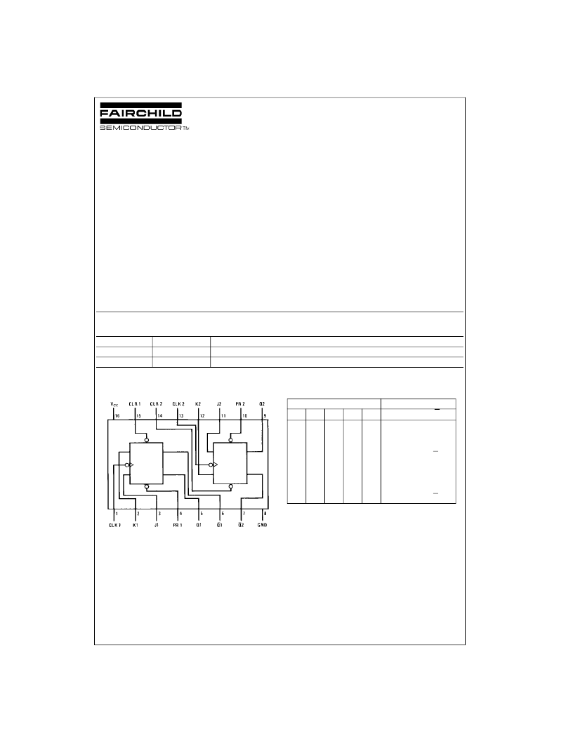
Connection Diagram
Function Table
H
=
HIGH Logic Level
L
=
LOW Logic Level
X
=
Either LOW or HIGH Logic Level
↓
=
Negative Going Edge of Pulse
Q
0
=
The output logic level before the indicated input conditions were
established.
Toggle
=
Each output changes to the complement of its previous level on
each falling edge of the clock pulse.
Note 1:
This configuration is nonstable; that is, it will not persist when
preset and/or clear inputs return to their inactive (HIGH) level.
Order Number
DM74KS112AM
DM74LS112AN
Package Number
M16A
N16E
Package Description
16-Lead Small Outline Integrated Circuit (SOIC), JEDEC MS-012, 0.150 Narrow
16-Lead Plastic Dual-In-Line Package (PDIP), JEDEC MS-001, 0.300 Wide
Inputs
Outputs
PR
L
H
L
H
H
H
H
CLR CLK
H
L
L
H
H
H
H
J
X
X
X
L
H
L
H
K
X
X
X
L
L
H
H
Q
H
L
Q
L
H
X
X
X
↓
↓
↓
↓
H
H (Note 1)
Q
0
H
L
H (Note 1)
Q
0
L
H
Toggle
H
H
X
X
Q
0
Q
0
相關PDF資料 |
PDF描述 |
|---|---|
| DM74LS112AN | Dual Negative-Edge-Triggered Master-Slave J-K Flip-Flop with Preset, Clear, and Complementary Outputs |
| DM74LS11M | Triple 3-Input AND Gate |
| DM74LS11 | Triple 3-Input AND Gate(三3輸入與門) |
| DM74LS11N | Triple 3-Input AND Gate |
| DM74LS11MX | Triple 3-input AND Gate |
相關代理商/技術參數(shù) |
參數(shù)描述 |
|---|---|
| DM74LS112A WAF | 制造商:Fairchild Semiconductor Corporation 功能描述: |
| DM74LS112AM | 功能描述:觸發(fā)器 Dl M-S J-K Flip-Flop RoHS:否 制造商:Texas Instruments 電路數(shù)量:2 邏輯系列:SN74 邏輯類型:D-Type Flip-Flop 極性:Inverting, Non-Inverting 輸入類型:CMOS 輸出類型: 傳播延遲時間:4.4 ns 高電平輸出電流:- 16 mA 低電平輸出電流:16 mA 電源電壓-最大:5.5 V 最大工作溫度:+ 85 C 安裝風格:SMD/SMT 封裝 / 箱體:X2SON-8 封裝:Reel |
| DM74LS112AMX | 功能描述:觸發(fā)器 Dl M-S J-K Flip-Flop RoHS:否 制造商:Texas Instruments 電路數(shù)量:2 邏輯系列:SN74 邏輯類型:D-Type Flip-Flop 極性:Inverting, Non-Inverting 輸入類型:CMOS 輸出類型: 傳播延遲時間:4.4 ns 高電平輸出電流:- 16 mA 低電平輸出電流:16 mA 電源電壓-最大:5.5 V 最大工作溫度:+ 85 C 安裝風格:SMD/SMT 封裝 / 箱體:X2SON-8 封裝:Reel |
| DM74LS112AN | 功能描述:觸發(fā)器 Dl M-S J-K Flip-Flop RoHS:否 制造商:Texas Instruments 電路數(shù)量:2 邏輯系列:SN74 邏輯類型:D-Type Flip-Flop 極性:Inverting, Non-Inverting 輸入類型:CMOS 輸出類型: 傳播延遲時間:4.4 ns 高電平輸出電流:- 16 mA 低電平輸出電流:16 mA 電源電壓-最大:5.5 V 最大工作溫度:+ 85 C 安裝風格:SMD/SMT 封裝 / 箱體:X2SON-8 封裝:Reel |
| DM74LS11M | 功能描述:邏輯門 Trp 3-Input AND Gate RoHS:否 制造商:Texas Instruments 產(chǎn)品:OR 邏輯系列:LVC 柵極數(shù)量:2 線路數(shù)量(輸入/輸出):2 / 1 高電平輸出電流:- 16 mA 低電平輸出電流:16 mA 傳播延遲時間:3.8 ns 電源電壓-最大:5.5 V 電源電壓-最小:1.65 V 最大工作溫度:+ 125 C 安裝風格:SMD/SMT 封裝 / 箱體:DCU-8 封裝:Reel |
發(fā)布緊急采購,3分鐘左右您將得到回復。