- 您現(xiàn)在的位置:買(mǎi)賣(mài)IC網(wǎng) > PDF目錄375723 > FAN5066MTC (FAIRCHILD SEMICONDUCTOR CORP) PDF資料下載
參數(shù)資料
| 型號(hào): | FAN5066MTC |
| 廠(chǎng)商: | FAIRCHILD SEMICONDUCTOR CORP |
| 元件分類(lèi): | 穩(wěn)壓器 |
| 中文描述: | SWITCHING CONTROLLER, 1000 kHz SWITCHING FREQ-MAX, PDSO20 |
| 封裝: | TSSOP-20 |
| 文件頁(yè)數(shù): | 12/18頁(yè) |
| 文件大小: | 263K |
| 代理商: | FAN5066MTC |
第1頁(yè)第2頁(yè)第3頁(yè)第4頁(yè)第5頁(yè)第6頁(yè)第7頁(yè)第8頁(yè)第9頁(yè)第10頁(yè)第11頁(yè)當(dāng)前第12頁(yè)第13頁(yè)第14頁(yè)第15頁(yè)第16頁(yè)第17頁(yè)第18頁(yè)
FAN5066
PRODUCT SPECIFICATION
12
REV. 2.1.4 11/13/01
In general, a higher operating frequency decreases the peak
ripple current flowing in the output inductor, thus allowing
the use of a smaller inductor value. In addition, operation at
higher frequencies decreases the amount of energy storage
that must be provided by the bulk output capacitors during
load transients due to faster loop response of the controller.
Unfortunately, the efficiency losses due to switching of the
MOSFETs increase as the operating frequency is increased.
Thus, efficiency is optimized at lower frequencies. An oper-
ating frequency of 300KHz is a typical choice which opti-
mizes efficiency and minimizes component size while
maintaining excellent regulation and transient performance
under all operating conditions.
Design Considerations and Component
Selection
Additional information on design and component selection
may be found in Fairchild Semiconductor’s Application
Note 53.
MOSFET Selection
This application requires N-channel Logic Level Enhance-
ment Mode Field Effect Transistors. Desired characteristics
are as follows:
Low Static Drain-Source On-Resistance,
R
DS,ON
< 20m
(lower is better)
Low gate drive voltage, V
GS
= 4.5V rated
Power package with low Thermal Resistance
Drain-Source voltage rating > 15V.
The on-resistance (R
DS,ON
) is the primary parameter for
MOSFET selection. The on-resistance determines the power
dissipation within the MOSFET and therefore significantly
affects the efficiency of the DC-DC Converter. For details
and a spreadsheet on MOSFET selection, refer to Applica-
tions Bulletin AB-8
MOSFET Gate Bias
The high side MOSFET gate driver can be biased by one of
two methods–Charge Pump or 12V Gate Bias. The charge
pump method has the advantage of requiring only +5V as an
input voltage to the converter, but the 12V method will real-
ize increased efficiency by providing an increased V
GS
to the
high side MOSFETs.
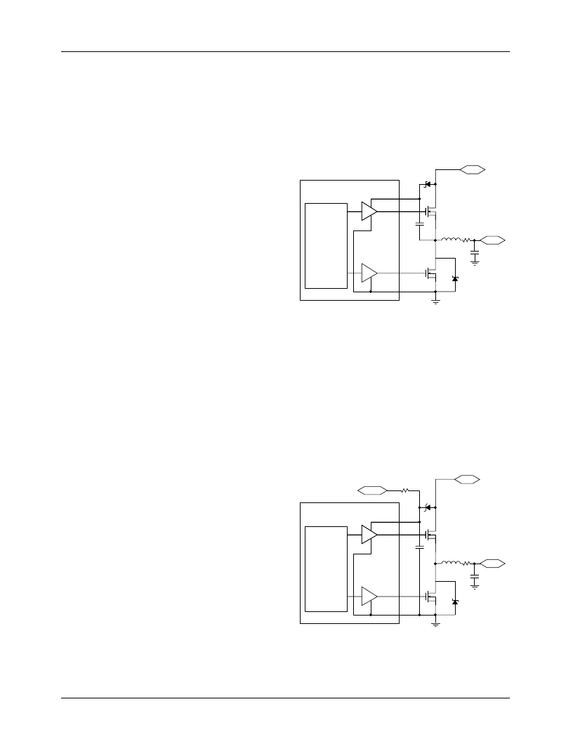
Method 1. Charge Pump (Bootstrap)
Figure 4 shows the use of a charge pump to provide gate bias
to the high side MOSFET when +12V is unavailable. Capac-
itor CP is the charge pump used to boost the voltage of the
FAN5066 output driver. When the MOSFET Q1 switches
off, the source of the MOSFET is at approximately 0V
because of the MOSFET Q2. (The Schottky D2 conducts for
only a very short time, and is not relevent to this discussion.)
CP is charged through the Schottky diode D1 to approxi-
mately 4.5V. When the MOSFET Q1 turns on, the voltage at
the source of the MOSFET is equal to 5V. The capacitor
voltage follows, and hence provides a voltage at VCCQP
equal to almost 10V. The Schottky diode D1 is required to
provide the charge path when the MOSFET is off, and
reverses biases when VCCQP goes to 10V. The charge pump
capacitor (CP) needs to be a high Q, high frequency capaci-
tor. A 1
μ
F ceramic capacitor is recommended here.
Figure 4. Charge Pump Configuration
Method 2. 12V Gate Bias
Figure 5 illustrates how a 12V source can be used to bias
VCCQP. A 47
resistor is used to limit the transient current
into the VCCQP pin and a 1μF capacitor is used to filter the
VCCQP supply. This method provides a higher gate bias
voltage (V
GS
) to the high side MOSFET than the charge
pump method, and therefore reduces the R
DS,ON
and the
resulting power loss within the MOSFET. In designs where
efficiency is a primary concern, the 12V gate bias method is
recommended. A 6.2V Zener diode, D1, is used to clamp the
voltage at VCCQP to a maximum of 12V and ensure that the
absolute maximum voltage of the IC will not be exceeded.
Figure 5. Gate Bias Configuration
PWM/PFM
Control
VO
+5V
D1
D2
CP
Q1
Q2
L2
RS
C
OUT
VCCQP
HIDRV
LODRV
GNDP
PWM/PFM
Control
VO
+5V
+12V
D2
1
μ
F
Q1
Q2
L2
RS
47
D1
VCCQP
HIDRV
LODRV
GNDP
C
OUT
相關(guān)PDF資料 |
PDF描述 |
|---|---|
| FAN5066MTCX | |
| FAN5067 | ACPI Dual Switch Controller |
| FAN5068MPX | DDR-1/DDR-2 plus ACPI Regulator Combo |
| FAN5068 | DDR-1/DDR-2 plus ACPI Regulator Combo |
| FAN5068ACPI | FAN5068 Component calculation and simulation tools |
相關(guān)代理商/技術(shù)參數(shù) |
參數(shù)描述 |
|---|---|
| FAN5066MTC_Q | 功能描述:開(kāi)關(guān)變換器、穩(wěn)壓器與控制器 DC/DC RoHS:否 制造商:Texas Instruments 輸出電壓:1.2 V to 10 V 輸出電流:300 mA 輸出功率: 輸入電壓:3 V to 17 V 開(kāi)關(guān)頻率:1 MHz 工作溫度范圍: 安裝風(fēng)格:SMD/SMT 封裝 / 箱體:WSON-8 封裝:Reel |
| FAN5066MTCX | 功能描述:開(kāi)關(guān)變換器、穩(wěn)壓器與控制器 DC-DC Controller ULV Synchronous RoHS:否 制造商:Texas Instruments 輸出電壓:1.2 V to 10 V 輸出電流:300 mA 輸出功率: 輸入電壓:3 V to 17 V 開(kāi)關(guān)頻率:1 MHz 工作溫度范圍: 安裝風(fēng)格:SMD/SMT 封裝 / 箱體:WSON-8 封裝:Reel |
| FAN5066MX | 功能描述:DC/DC 開(kāi)關(guān)控制器 DC-DC Controller ULV Synchronous RoHS:否 制造商:Texas Instruments 輸入電壓:6 V to 100 V 開(kāi)關(guān)頻率: 輸出電壓:1.215 V to 80 V 輸出電流:3.5 A 輸出端數(shù)量:1 最大工作溫度:+ 125 C 安裝風(fēng)格: 封裝 / 箱體:CPAK |
| FAN5067 | 制造商:FAIRCHILD 制造商全稱(chēng):Fairchild Semiconductor 功能描述:ACPI Dual Switch Controller |
| FAN5067M | 功能描述:開(kāi)關(guān)變換器、穩(wěn)壓器與控制器 aCPI Dual Switch Controller RoHS:否 制造商:Texas Instruments 輸出電壓:1.2 V to 10 V 輸出電流:300 mA 輸出功率: 輸入電壓:3 V to 17 V 開(kāi)關(guān)頻率:1 MHz 工作溫度范圍: 安裝風(fēng)格:SMD/SMT 封裝 / 箱體:WSON-8 封裝:Reel |
發(fā)布緊急采購(gòu),3分鐘左右您將得到回復(fù)。