- 您現在的位置:買賣IC網 > PDF目錄375724 > FAN5231 (FAIRCHILD SEMICONDUCTOR CORP) Micropower 5V, 100mA Low Dropout Linear Regulator PDF資料下載
參數資料
| 型號: | FAN5231 |
| 廠商: | FAIRCHILD SEMICONDUCTOR CORP |
| 元件分類: | 穩壓器 |
| 英文描述: | Micropower 5V, 100mA Low Dropout Linear Regulator |
| 中文描述: | 1 A SWITCHING REGULATOR, 345 kHz SWITCHING FREQ-MAX, PDSO28 |
| 封裝: | QSOP-28 |
| 文件頁數: | 7/17頁 |
| 文件大小: | 360K |
| 代理商: | FAN5231 |
FAN5231
REV. 1.1.1 8/15/01
7
Description
Operation Overview
The FAN5231 three-in-one power mangement integrated
circuit provides complete power solution for modern proces-
sors for notebook and sub-notebook PCs. The IC controls
operation of two synchronous buck converters and one linear
regulator. The output voltage of the core converter can be
adjusted in the range from 0.925V to 2.0 by changing the
DAC code settings (see Table 1). The output voltage of the
I/O converter is fixed to 1.5V. The internal linear regulator
provides fixed 2.5V for the CPU clock generator from the
system +3.3V bus. The output voltage of the core converter
can be changed on-the-fly with programable slew rate, which
makes it especially suitable for the processors that feature
modern power savings techniques as SpeedStep or Power-
Now! .
Both, core and I/O converters can operate in two modes:
fixed frequency PWM and variable frequency hysteretic
depending on the load level. At loads lower than the critical
where filter inductor current becomes discontinuous, hyster-
etic mode of operation is activated. Switchover from PWM
to hysteretic operation at light loads improves the converters'
efficiency and prolongs battery run time. In hysteretic mode,
comparators are synchronized to the main clock that allows
seamless transition between the operational modes and
reduced channel-to-channel interaction. As the filter inductor
resumes continuous current, the PWM mode of operation is
restored.
The core converter incorporates a proprietary output voltage
droop circuit for optimum handling of the fast load transients
found in modern processors. The droop is compensated for
the processor mode changes, which allows for relatively
equal droop in any operation mode and to specify the droop
as a fraction of the VID set voltage.
Initialization
The FAN5231 initializes upon receipt of input power assum-
ing EN is high or not connected. The Power-On Reset (POR)
function continually monitors the input supply voltage on the
VCC pin and initiates soft-start operation after input supply
voltage exceeds 4.5V. Should this voltage drop lower than
4.0V, POR disables the chip.
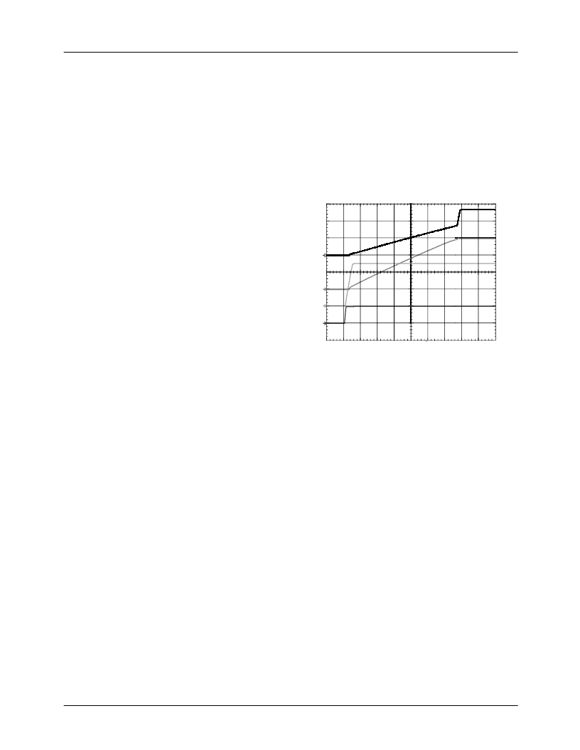
Soft-Start
When soft start is initiated, the voltage on the SOFT pin
starts to ramp gradually due to the 25μA current sourced into
the external capacitor.
When SOFT-pin voltage reaches 0.9V, the value of the sourc-
ing current rapidly changes to 500μA charging the soft-start
capacitor to the level determined by the DAC. This completes
the soft start sequence, Fig. 2. As long as the SOFT voltage is
above 0.9V, the maximum value of the internal soft-start cur-
rent is set to 500μA allowing fast rate-of-change in the core
output voltage due to a VID code change.
In this mode SOFT has both sourcing and sinking capabili-
ties to maintain voltage across the soft-start capacitor con-
forming to the VID code.
This dual slope approach helps to provide safe rise of volt-
ages and currents in the converters during initial start-up and
at the same time sets a controlled speed of the core voltage
change when the processor commands to do so.
Soft-start circuits for the I/O converter is slaved to the core
output soft-start circuit and they complete their ramp-up
when voltage on the SOFT pin reaches 0.9V.
Figure 2. Initial Startup
The value of the soft-start capacitor can be estimated by the
following equation:
For the typical conditions when
Vdac = 0.25V,
t = 100μs
With this value of the soft-start capacitor, soft start time will
be equal to:
OUT1 Voltage Program
This output of PWM1 converter is designated to supply
the microprocessor core voltage. The OUT1 voltage is
programmed to discrete levels between 0.925V
DC
and
2.0V
DC
as specified in Table 1. The voltage identification
(VID) pins program an internal voltage reference (DAC)
through a TTL-compatible 5-bit digital-to-analog converter.
The level of the DAC voltage also sets the PGOOD, UVP
and OVP thresholds. The VID pins can be left open for a
logic 1 input due to an internal 1μA pull-up to Vcc.
(3) Ch3 V
CLK
1.0V
(2) Ch2 V
IO
500mV
(4) Ch4 V
EN
5.0V
M1.00ms
V
IN
= 20V
(1) Ch1 V
CPU
500mV
1
2
3
4
Css
Vdac
----------------
t
=
Css
μ
A
0.25
V
500
μ
s
0.2
μ
F
≈
=
Tss
μ
F
0.2
0.9
V
25
μ
A
7.2
ms
=
=
相關PDF資料 |
PDF描述 |
|---|---|
| FAN5231QSC | Analog IC |
| FAN5232 | Adjustable PWM Buck Controller for LCD PCs |
| FAN5232MTC | SMPS Controller |
| FAN5233 | System Electronics Regulator for Mobile PCs |
| FAN5233MTC | Analog IC |
相關代理商/技術參數 |
參數描述 |
|---|---|
| FAN5231 WAF | 制造商:Fairchild Semiconductor Corporation 功能描述: |
| FAN5231QSC | 功能描述:開關變換器、穩壓器與控制器 QSOP-28 RoHS:否 制造商:Texas Instruments 輸出電壓:1.2 V to 10 V 輸出電流:300 mA 輸出功率: 輸入電壓:3 V to 17 V 開關頻率:1 MHz 工作溫度范圍: 安裝風格:SMD/SMT 封裝 / 箱體:WSON-8 封裝:Reel |
| FAN5231QSCX | 功能描述:開關變換器、穩壓器與控制器 QSOP-28 RoHS:否 制造商:Texas Instruments 輸出電壓:1.2 V to 10 V 輸出電流:300 mA 輸出功率: 輸入電壓:3 V to 17 V 開關頻率:1 MHz 工作溫度范圍: 安裝風格:SMD/SMT 封裝 / 箱體:WSON-8 封裝:Reel |
| FAN5232 | 制造商:FAIRCHILD 制造商全稱:Fairchild Semiconductor 功能描述:Adjustable PWM Buck Controller for LCD PCs |
| FAN5232_CBC3116B WAF | 制造商:Fairchild Semiconductor Corporation 功能描述: |
發布緊急采購,3分鐘左右您將得到回復。