- 您現在的位置:買賣IC網 > Datasheet目錄38 > FAN7930BM (Fairchild Semiconductor)IC PFC CTLR CRITICAL CONF 8-SOIC Datasheet資料下載
參數資料
| 型號: | FAN7930BM |
| 廠商: | Fairchild Semiconductor |
| 文件頁數: | 13/22頁 |
| 文件大小: | 1849K |
| 描述: | IC PFC CTLR CRITICAL CONF 8-SOIC |
| 標準包裝: | 95 |
| 模式: | 臨界傳導(CRM) |
| 頻率 - 開關: | 250kHz ~ 350kHz |
| 電流 - 啟動: | 120µA |
| 電源電壓: | 13 V ~ 20 V |
| 工作溫度: | -40°C ~ 125°C |
| 安裝類型: | 表面貼裝 |
| 封裝/外殼: | 8-SOIC(0.154",3.90mm 寬) |
| 供應商設備封裝: | 8-SOP |
| 包裝: | 管件 |
?2010 Fairchild Semiconductor Corporation
www.fairchildsemi.com
FAN7930B " Rev. 1.0.3
13
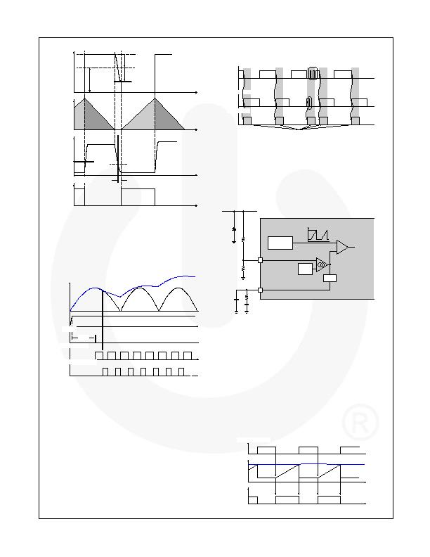
Figure 28. Auxiliary Voltage Threshold
When no ZCD signal is available, the PFC controller
cannot turn on the MOSFET, so the controller checks
every switching off time and forces MOSFET turn on
when the off time is longer than 150 約. This restart
timer triggers MOSFET turn-on at startup and may be
used at the input voltage zero cross period.
Figure 29. Restart Timer at Startup
Because the MOSFET turn-on depends on the ZCD
input, switching frequency may increase to higher than
several megahertz due to the mis-triggering or noise on
the nearby ZCD pin. If the switching frequency is higher
than needed for critical conduction mode (CRM),
operation mode shifts to continuous conduction mode
(CCM). In CCM, unlike CRM where the boost inductor
current is reset to zero at the next switch on; inductor
current builds up at every switching cycle and can be
raised to very high current that exceeds the current
rating of the power switch or diode. This can seriously
damage the power switch. To avoid this, maximum
switching frequency limitation is embedded. If ZCD
signal is applied again within 3.3 約 after the previous
rising edge of gate signal, this signal is ignored
internally and FAN7930B waits for another ZCD signal.
This slightly degrades the power factor performance at
light load and high input voltage.
ZC D
a f t e r C O M P A R A T O R
M O S F E T G a t e
M a x f
S W
L i m i t
In h i i R i n
E r r o r O c c u r s !
I g n o r e s Z C D N o i s e
t
Figure 30. Maximum Switching Frequency
Limit Operation
6. Control: The scaled output is compared with the
internal reference voltage and sinking or sourcing
current is generated from the COMP pin by the
transconductance amplifier. The error amplifier output is
compared with the internal sawtooth waveform to give
proper turn-on time based on the controller.
V
O U T
P F C
+
-
IN V
1
C O M P
3
C la m p
C ir c u it
+
-
V
RE F
S ta ir
S te p
T H D o p tim iz e d
S a w to o th
G e n e r a to r
S a w t o o t h
M O S F E T O f f
R 1
C 1
C 2
1V
6 . 2 V
Figure 31. Control Circuit
Unlike a conventional voltage-mode PWM controller,
FAN7930B turns on the MOSFET at the falling edge of
ZCD signal. The
ON
instant is determined by the
external signal and the turn-on time lasts until the error
amplifier output (V
COMP
) and sawtooth waveform meet.
When load is heavy, output voltage decreases, scaled
output decreases, COMP voltage increases to
compensate low output, turn-on time lengthens to give
more inductor turn-on time, and increased inductor
current raises the output voltage. This is how a PFC
negative feedback controller regulates output.
The maximum of V
COMP
is limited to 6.5 V, which
dictates the maximum turn-on time. Switching stops
when V
COMP
is lower than 1.0 V.
Z C D
a f t e r C O M P A R A T O R
V CO M P & S a w t o o t h
M O S F E T G a t e
V
1
.
Figure 32. Turn-On Time Determination
D
相關PDF資料 |
PDF描述 |
|---|---|
| FAN7930CM | IC PFC CTLR CRITICAL CONF 8-SOIC |
| FAN9611MX | IC PFC CTLR DUAL BCM 16-SOIC |
| FAN9612MX | IC CTLR PFC DUAL BCM 16SOICN |
| FL6961MY | IC CTLR PFC SGL FLYBACK 8-SOIC |
| IR1150ISTRPBF | IC PFC CONTROLLER CCM 8-SOIC |
相關代理商/技術參數 |
參數描述 |
|---|---|
| FAN7930BMX | 功能描述:功率因數校正 IC Critical Conduction Mode PFC Controller RoHS:否 制造商:Fairchild Semiconductor 開關頻率:300 KHz 最大功率耗散: 最大工作溫度:+ 125 C 安裝風格:SMD/SMT 封裝 / 箱體:SOIC-8 封裝:Reel |
| FAN7930BMX_G | 制造商:Fairchild Semiconductor Corporation 功能描述:IC PFC CTLR CRITICAL CONF 8-SOIC 制造商:Fairchild Semiconductor Corporation 功能描述:Power Factor Correction - PFC Critical Conduction Mode PFC Controller 制造商:Fairchild Semiconductor Corporation 功能描述:Critical Conduction Mode PFC Controller |
| FAN7930C | 制造商:FAIRCHILD 制造商全稱:Fairchild Semiconductor 功能描述:The FAN7930C is an active power factor correction(PFC) controller for boost PFC applications that operate in critical conduction mode(CRM). |
| FAN7930CM | 功能描述:功率因數校正 IC Critical Conduction Mode PFC Controller RoHS:否 制造商:Fairchild Semiconductor 開關頻率:300 KHz 最大功率耗散: 最大工作溫度:+ 125 C 安裝風格:SMD/SMT 封裝 / 箱體:SOIC-8 封裝:Reel |
| FAN7930CMX | 功能描述:功率因數校正 IC Critical Conduction Mode PFC Controller RoHS:否 制造商:Fairchild Semiconductor 開關頻率:300 KHz 最大功率耗散: 最大工作溫度:+ 125 C 安裝風格:SMD/SMT 封裝 / 箱體:SOIC-8 封裝:Reel |
發布緊急采購,3分鐘左右您將得到回復。