- 您現在的位置:買賣IC網 > PDF目錄375763 > FDA15N65 (FAIRCHILD SEMICONDUCTOR CORP) 650V N-Channel MOSFET PDF資料下載
參數資料
| 型號: | FDA15N65 |
| 廠商: | FAIRCHILD SEMICONDUCTOR CORP |
| 元件分類: | JFETs |
| 英文描述: | 650V N-Channel MOSFET |
| 中文描述: | 16 A, 650 V, 0.44 ohm, N-CHANNEL, Si, POWER, MOSFET |
| 封裝: | TO-3 PIN |
| 文件頁數: | 1/8頁 |
| 文件大小: | 797K |
| 代理商: | FDA15N65 |
UniFET
TM
January 2007
200
7
Fairchild Semiconductor Corporation
FDA15N65 Rev. A
1
www.fairchildsemi.com
F
FDA15N65
650V N-Channel MOSFET
Features
16A, 650V, R
DS(on)
= 0.44
Ω
@V
GS
= 10 V
Low gate charge ( typical 48.5 nC)
Low C
rss
( typical 23.6 pF)
Fast switching
100% avalanche tested
Improved dv/dt capability
Description
These N-Channel enhancement mode power field effect
transistors are produced using Fairchild’s proprietary, planar
stripe, DMOS technology.
This advanced technology has been especially tailored to
minimize on-state resistance, provide superior switching
performance, and withstand high energy pulse in the avalanche
and commutation mode. These devices are well suited for high
efficient switched mode power supplies and active power factor
correction.
Absolute Maximum Ratings
Thermal Characteristics
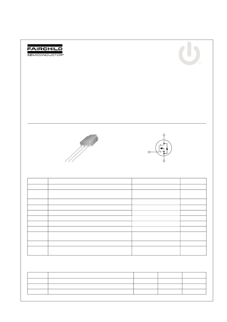
D
G
S
G
S
D
TO-3PN
FDA Series
Symbol
Parameter
FDA15N65
Unit
V
DSS
I
D
Drain-Source Voltage
650
V
Drain Current
- Continuous (T
C
= 25
°
C)
- Continuous (T
C
= 100
°
C)
- Pulsed
16
9.6
A
A
I
DM
Drain Current
(Note 1)
64
A
V
GSS
E
AS
I
AR
E
AR
dv/dt
Gate-Source voltage
±
30
V
Single Pulsed Avalanche Energy
(Note 2)
637
mJ
Avalanche Current
(Note 1)
16
A
Repetitive Avalanche Energy
(Note 1)
26
mJ
Peak Diode Recovery dv/dt
(Note 3)
4.5
V/ns
P
D
Power Dissipation
(T
C
= 25
°
C)
- Derate above 25
°
C
260
2.1
W
W/
°
C
T
J,
T
STG
T
L
Operating and Storage Temperature Range
-55 to +150
°
C
Maximum Lead Temperature for Soldering Purpose,
1/8” from Case for 5 Seconds
300
°
C
Symbol
Parameter
Min.
Max.
Unit
R
θ
JC
R
θ
CS
R
θ
JA
Thermal Resistance, Junction-to-Case
--
0.48
°
C/W
Thermal Resistance, Case-to-Sink
0.24
--
°
C/W
Thermal Resistance, Junction-to-Ambient
--
40
°
C/W
相關PDF資料 |
PDF描述 |
|---|---|
| FDA16N50 | 500V N-Channel MOSFET |
| FDA16N50_07 | 500V N-Channel MOSFET |
| FDA16N50_F109 | 500V N-Channel MOSFET |
| FDA18N50 | 500V N-Channel MOSFET |
| FDA20N50 | 500V N-Channel MOSFET |
相關代理商/技術參數 |
參數描述 |
|---|---|
| FDA-15P0L2TI2/1-LF | 制造商:Cinch Connectors 功能描述:15 way Filter D Plug Straight Flow Solder |
| FDA15P-1064MTX | 制造商:SOURIAU 功能描述: |
| FDA15P-1164MTX | 制造商:SOURIAU 功能描述: |
| FDA15P-1264MTX | 制造商:SOURIAU 功能描述: |
| FDA15P-964MTX | 制造商:SOURIAU 功能描述: |
發布緊急采購,3分鐘左右您將得到回復。