- 您現在的位置:買賣IC網 > PDF目錄375769 > FDC6332L (FAIRCHILD SEMICONDUCTOR CORP) Common Source Load Switch P-Channel 1.8V Specified PowerTrench MOSFET PDF資料下載
參數資料
| 型號: | FDC6332L |
| 廠商: | FAIRCHILD SEMICONDUCTOR CORP |
| 元件分類: | 外設及接口 |
| 英文描述: | Common Source Load Switch P-Channel 1.8V Specified PowerTrench MOSFET |
| 中文描述: | 1 A BUF OR INV BASED PRPHL DRVR, PDSO6 |
| 封裝: | SUPER SOT-6 |
| 文件頁數: | 2/4頁 |
| 文件大小: | 149K |
| 代理商: | FDC6332L |
FDC6332L Rev D(W)
Electrical Characteristics
T
A
= 25°C unless otherwise noted
Test Conditions
Symbol
Parameter
Min
Typ
Max Units
Off Characteristics
BV
IN
IR
IN
BVG
OFF
I
GOFF
Input – Output Breakdown Voltage
Reverse Input Current
Driver FET Gate Breakdown Voltage
Driver FET Gate Leakage Current
V
ON/OFF
= 0 V,
V
IN
= –8V,
I
G
= 250uA
V
G
= 8 V
I
D
= –250
μ
A
V
ON/OFF
= 0 V
–20
8
V
μ
A
V
nA
–1
100
On Characteristics
V
IN
V
ON
V
OFF
I
LOAD
R
DS(on)
(Note 2)
Input Voltage Range
Turn-On Voltage Range
Turn-off Voltage Range
Output Load Current
Static Drain–Source
On–Resistance
V
IN
= –5 V
V
GS
= 4.5 V,
V
GS
= 2.5 V,
V
GS
= 1.8 V,
V
IN
= 8 V,
V
IN
= 8 V,
V
IN
= 8 V,
1.8
1.5
–0.2
–1
2.5
230
338
643
409
411
420
8
8
0.2
350
500
750
V
V
V
A
m
m
V
ON
= –4.5V
I
D
= –1.0A
I
D
= –0.9 A
I
D
= –0.7 A
I
D
= –1.0 A
I
D
= –0.9 A
I
D
= –0.7 A
R
ON
Loadswitch On-Resistance
Drain–Source Diode Characteristics and Maximum Ratings
I
S
Maximum Continuous Drain–Source Diode Forward Current
V
SD
Drain–Source Diode Forward Voltage
–0.6
–1.2
A
V
V
ON/OFF
= 0 V, I
S
= –0.6 A
(Note 2
–0.9
Notes:
1.
R
θ
JA
is the sum of the junction-to-case and case-to-ambient thermal resistance where the case thermal reference is defined as the solder mounting surface of
the drain pins. R
θ
JC
is guaranteed by design while R
θ
CA
is determined by the user's board design.
a)
90°C/W when
mounted on a 1in
2
pad
of 2 oz copper
b)
160°C/W when mounted
on a minimum pad of 2 oz
copper
Scale 1 : 1 on letter size paper
2.
Pulse Test: Pulse Width < 300
μ
s, Duty Cycle < 2.0%
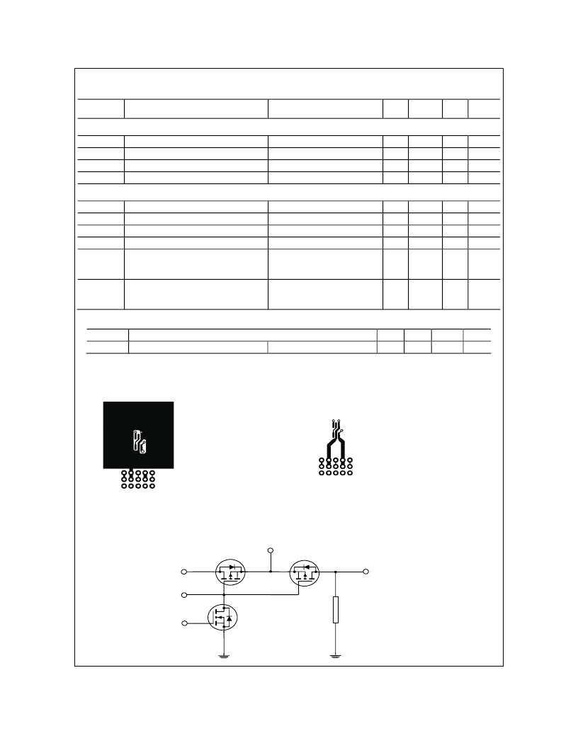
FDC6332L Load Switch Application Circuit
F
Q2
IN
G1/G2
OUT
ON/OFF
LOAD
Q3
Q1
S1/S2
相關PDF資料 |
PDF描述 |
|---|---|
| FDC6333C | 30V N & P-Channel PowerTrench MOSFETs |
| FDC633N | N-Channel Enhancement Mode Field Effect Transistor(P溝道增強型MOS場效應晶體管) |
| FDC634 | P-Channel Enhancement Mode Field Effect Transistor |
| FDC634P | P-Channel Enhancement Mode Field Effect Transistor(P溝道增強型MOS場效應晶體管) |
| FDC636P | P-Channel Logic Level Enhancement Mode Field Effect Transistor |
相關代理商/技術參數 |
參數描述 |
|---|---|
| FDC6332L_Q | 功能描述:MOSFET 1.8V P-Ch MOSFET Common Source RoHS:否 制造商:STMicroelectronics 晶體管極性:N-Channel 汲極/源極擊穿電壓:650 V 閘/源擊穿電壓:25 V 漏極連續(xù)電流:130 A 電阻汲極/源極 RDS(導通):0.014 Ohms 配置:Single 最大工作溫度: 安裝風格:Through Hole 封裝 / 箱體:Max247 封裝:Tube |
| FDC6333C | 功能描述:MOSFET 30V/-30V N/P RoHS:否 制造商:STMicroelectronics 晶體管極性:N-Channel 汲極/源極擊穿電壓:650 V 閘/源擊穿電壓:25 V 漏極連續(xù)電流:130 A 電阻汲極/源極 RDS(導通):0.014 Ohms 配置:Single 最大工作溫度: 安裝風格:Through Hole 封裝 / 箱體:Max247 封裝:Tube |
| FDC6333C | 制造商:Fairchild Semiconductor Corporation 功能描述:MOSFET NP CH 30V 2.5/2A SSOT6 制造商:Fairchild Semiconductor Corporation 功能描述:MOSFET, NP CH, 30V, 2.5/2A, SSOT6 制造商:Fairchild Semiconductor Corporation 功能描述:MOSFET, NP CH, 30V, 2.5/2A, SSOT6; Transistor Polarity:N and P Channel; Continuous Drain Current Id:2.5A; Drain Source Voltage Vds:30V; On Resistance Rds(on):95mohm; Rds(on) Test Voltage Vgs:10V; Threshold Voltage Vgs Typ:1.8V ;RoHS Compliant: Yes |
| FDC6333C | 制造商:Fairchild Semiconductor Corporation 功能描述:MOSFET TRANSISTOR 制造商:Fairchild Semiconductor Corporation 功能描述:DUAL N/P CH MOSFET, 30V SUPER SOT-6 |
| FDC6333C_Q | 功能描述:MOSFET 30V/-30V N/P RoHS:否 制造商:STMicroelectronics 晶體管極性:N-Channel 汲極/源極擊穿電壓:650 V 閘/源擊穿電壓:25 V 漏極連續(xù)電流:130 A 電阻汲極/源極 RDS(導通):0.014 Ohms 配置:Single 最大工作溫度: 安裝風格:Through Hole 封裝 / 箱體:Max247 封裝:Tube |
發(fā)布緊急采購,3分鐘左右您將得到回復。