- 您現在的位置:買賣IC網 > PDF目錄375777 > FDMF8700 (FAIRCHILD SEMICONDUCTOR CORP) Driver plus FET Multi-chip Module PDF資料下載
參數資料
| 型號: | FDMF8700 |
| 廠商: | FAIRCHILD SEMICONDUCTOR CORP |
| 元件分類: | MOSFETs |
| 英文描述: | Driver plus FET Multi-chip Module |
| 中文描述: | HALF BRDG BASED MOSFET DRIVER, QCC56 |
| 封裝: | 8 X 8 MM, ROHS COMPLIANT, MO-220WLLD-5, SMD-56 |
| 文件頁數: | 11/13頁 |
| 文件大小: | 563K |
| 代理商: | FDMF8700 |
11
www.fairchildsemi.com
FDMF8700 Rev. C3
F
Module Power Loss Measurement and
Calculation
Refer to Figure 27 for module power loss testing method. Power
loss calculation are as follows:
(a) P
IN
(b) P
OUT
(c) P
LOSS
= (V
IN
x I
IN
) + (V
CIN
x I
CIN
) (W)
= V
O
x I
OUT
(W)
= P
IN
- P
OUT
(W)
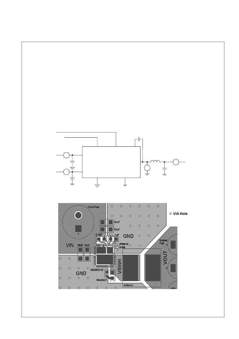
PCB Layout Guideline
Figure 28. shows a proper layout example of FDMF8700 and
critical parts. All of high current flow path, such as V
IN
, VSWH,
V
OUT
and GND copper, should be short and wide for better and
stable current flow, heat radiation and system performance.
Following is a guideline which the PCB designer should
consider:
1. Input bypass capacitors should be close to V
IN
and GND pin
of FDMF8700 to help reduce input current ripple component
induced by switching operation.
2. It is critical that the VSWH copper has minimum area for
lower switching noise emission. VSWH copper trace should
also be wide enough for high current flow. Other signal routing
path, such as PWM IN and BOOT signal, should be considered
with care to avoid noise pickup from VSWH copper area.
3. Output inductor location should be as close as possible to the
FDMF8700 for lower power loss due to copper trace.
4. Place ceramic bypass capacitor and boot capacitor as close
to VCIN and BOOT pin of FDMF8700 in order to supply stable
power. Routing width and length should also be considered.
5. Use multiple Vias on each copper area to interconnect each
top, inner and bottom layer to help smooth current flow and heat
conduction. Vias should be relatively large and of reasonable
inductance.
Figure 27. Power Loss Measurement Block Diagram
Figure 28. Typical PCB Layout Example (Top View)
I
IN
A
PWM input
PWM
BOOT
V
IN
PGND
V
SWH
FDMF8700
CGND
C
BOOT
I
OUT
A
L
VOUT
V V
O
DISB
DISB
VIN
I
CIN
A
V
CIN
VCIN
C
VCIN
C
VIN
IC Ground
Power Ground
C
OUT
相關PDF資料 |
PDF描述 |
|---|---|
| FDMF8704 | High Current / High Frequency FET plus Driver Multi-chip Module |
| FDMF8705 | Driver plus FET Multi-chip Module |
| FDMJ1023PZ | Dual P-Channel PowerTrench㈢ MOSFET |
| FDMS2380 | 740; 38000/740 Series; Microcontroller; Bit Size: 8-bit; ROM: 2K; RAM: 192; ROM Type: QzROM; CPU: 740 core; Minimum Instruction Execution Time (ns): 250 (@8MHz); Operating Frequency / Supply Voltage: 1.8 to 5.5V; Operating Ambient Temperature (°C): -20 to 85; Package Code: PLSP0020JB-A (20P2F-A) |
| FDMS2572_07 | N-Channel UltraFET Trench㈢ MOSFET 150V, 27A, 47mз |
相關代理商/技術參數 |
參數描述 |
|---|---|
| FDMF8704 | 功能描述:功率驅動器IC Driver plus FET Multi-chip Module RoHS:否 制造商:Micrel 產品:MOSFET Gate Drivers 類型:Low Cost High or Low Side MOSFET Driver 上升時間: 下降時間: 電源電壓-最大:30 V 電源電壓-最小:2.75 V 電源電流: 最大功率耗散: 最大工作溫度:+ 85 C 安裝風格:SMD/SMT 封裝 / 箱體:SOIC-8 封裝:Tube |
| FDMF8704V | 功能描述:功率驅動器IC Driver plus FET w/5v reg RoHS:否 制造商:Micrel 產品:MOSFET Gate Drivers 類型:Low Cost High or Low Side MOSFET Driver 上升時間: 下降時間: 電源電壓-最大:30 V 電源電壓-最小:2.75 V 電源電流: 最大功率耗散: 最大工作溫度:+ 85 C 安裝風格:SMD/SMT 封裝 / 箱體:SOIC-8 封裝:Tube |
| FDMF8705 | 功能描述:功率驅動器IC MLP 8X8 DRIVER PLUS FET MULTI-CHIP MODU RoHS:否 制造商:Micrel 產品:MOSFET Gate Drivers 類型:Low Cost High or Low Side MOSFET Driver 上升時間: 下降時間: 電源電壓-最大:30 V 電源電壓-最小:2.75 V 電源電流: 最大功率耗散: 最大工作溫度:+ 85 C 安裝風格:SMD/SMT 封裝 / 箱體:SOIC-8 封裝:Tube |
| FDMH000C11L-YW | 制造商:Thomas & Betts 功能描述:HAZ3FLD,1000W,M.H.,5 TAP BALST |
| FDMHP17C070-YWE | 制造商:Thomas & Betts 功能描述:HZ FDMHP17C070YWE HAZ3,FLD,175W,M.H |
發布緊急采購,3分鐘左右您將得到回復。