- 您現在的位置:買賣IC網 > PDF目錄375783 > FDS6900AS (FAIRCHILD SEMICONDUCTOR CORP) Dual N-Ch PowerTrench SyncFET PDF資料下載
參數資料
| 型號: | FDS6900AS |
| 廠商: | FAIRCHILD SEMICONDUCTOR CORP |
| 元件分類: | 小信號晶體管 |
| 英文描述: | Dual N-Ch PowerTrench SyncFET |
| 中文描述: | 8200 mA, 30 V, 2 CHANNEL, N-CHANNEL, Si, SMALL SIGNAL, MOSFET |
| 封裝: | SO-8 |
| 文件頁數: | 3/10頁 |
| 文件大小: | 183K |
| 代理商: | FDS6900AS |
FDS6900AS Rev
B
(X)
Electrical Characteristics
(continued)
Symbol
Switching Characteristics
(Note 2)
Q
g
(TOT)
Total Gate Charge at Vgs=10V
T
A
= 25°C unless otherwise noted
Parameter
Test Conditions
Type
Min
Typ
Max
Units
Q2
Q1
Q2
Q1
Q2
Q1
Q2
Q1
10
11
5.8
6.1
1.6
1.7
2.1
2.2
15
15
8.2
8.5
nC
nC
nC
nC
Q
g
Total Gate Charge at Vgs=5V
Q
gs
Gate–Source Charge
Q
gd
Gate–Drain Charge
Q2:
V
DS
= 15 V, I
D
= 8.2A
Q1:
V
DS
= 15 V, I
D
= 6.9A
Drain–Source Diode Characteristics and Maximum Ratings
I
S
Maximum Continuous Drain-Source Diode Forward Current
Q2
Q1
Q2
2.3
1.3
A
ns
T
rr
Q
rr
T
rr
Q
rr
V
SD
Reverse Recovery Time
Reverse Recovery Charge
Reverse Recovery Time
Reverse Recovery Charge
Drain-Source Diode Forward
Voltage
15
6
19
10
0.6
0.7
0.7
I
F
= 8.2 A,
d
iF
/d
t
= 300 A/μs
(Note 3)
nC
ns
I
F
= 6.9 A,
d
iF
/d
t
= 100 A/μs
(Note 3)
Q1
nC
V
V
GS
= 0 V, I
S
= 2.3 A
(Note 2)
V
GS
= 0 V, I
S
= 5 A
(Note 2)
V
GS
= 0 V, I
S
= 1.3 A
(Note 2)
Q2
Q2
Q1
0.7
1.0
1.2
Notes:
1.
R
θ
JA
is the sum of the junction-to-case and case-to-ambient thermal resistance where the case thermal reference is defined as the solder mounting surface of
the drain pins. R
θ
JC
is guaranteed by design while R
θ
CA
is determined by the user's board design.
a)
78°C/W when
mounted on a
0.5in
2
pad of 2
oz copper
b)
125°C/W when
mounted on a
0.02 in
2
pad of
2 oz copper
c)
135°C/W when
mounted on a
minimum pad.
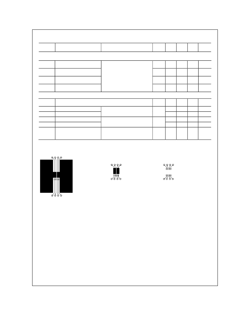
Scale 1 : 1 on letter size paper
2.
Pulse Test: Pulse Width < 300
μ
s, Duty Cycle < 2.0%
3.
See “SyncFET Schottky body diode characteristics” below.
4.
FDS6900AS_NL is a lead free product. The FDS6900AS_NL marking will appear on the reel label.
F
相關PDF資料 |
PDF描述 |
|---|---|
| FDS6900AS_NL | Dual N-Ch PowerTrench SyncFET |
| FDS6900S | Dual N-Ch PowerTrench SyncFet⑩ |
| FDS6910 | Dual N-Channel Logic Level PowerTrench MOSFET |
| FDS6912A | Dual N-Channel, Logic Level, PowerTrenchTM MOSFET |
| FDS6912 | Dual N-Channel Logic Level PWM Optimized PowerTrench MOSFET |
相關代理商/技術參數 |
參數描述 |
|---|---|
| FDS6900AS_NL | 制造商:FAIRCHILD 制造商全稱:Fairchild Semiconductor 功能描述:Dual N-Ch PowerTrench SyncFET |
| FDS6900S | 功能描述:MOSFET Dual NCh PowerTrench RoHS:否 制造商:STMicroelectronics 晶體管極性:N-Channel 汲極/源極擊穿電壓:650 V 閘/源擊穿電壓:25 V 漏極連續電流:130 A 電阻汲極/源極 RDS(導通):0.014 Ohms 配置:Single 最大工作溫度: 安裝風格:Through Hole 封裝 / 箱體:Max247 封裝:Tube |
| FDS6910 | 功能描述:MOSFET Dual N-Ch LogicLevel PowerTrench MOSFET RoHS:否 制造商:STMicroelectronics 晶體管極性:N-Channel 汲極/源極擊穿電壓:650 V 閘/源擊穿電壓:25 V 漏極連續電流:130 A 電阻汲極/源極 RDS(導通):0.014 Ohms 配置:Single 最大工作溫度: 安裝風格:Through Hole 封裝 / 箱體:Max247 封裝:Tube |
| FDS6910-CUT TAPE | 制造商:FAIRCHILD 功能描述:FDS6910 Series 30V 13 mOhm Dual N-Channel Logic Level PowerTrench Mosfet- SOIC-8 |
| FDS6911 | 功能描述:MOSFET LOW_VOLTAGE RoHS:否 制造商:STMicroelectronics 晶體管極性:N-Channel 汲極/源極擊穿電壓:650 V 閘/源擊穿電壓:25 V 漏極連續電流:130 A 電阻汲極/源極 RDS(導通):0.014 Ohms 配置:Single 最大工作溫度: 安裝風格:Through Hole 封裝 / 箱體:Max247 封裝:Tube |
發布緊急采購,3分鐘左右您將得到回復。