- 您現在的位置:買賣IC網 > PDF目錄375784 > FDS6984AS (FAIRCHILD SEMICONDUCTOR CORP) Dual Notebook Power Supply N-Channel PowerTrench SyncFET PDF資料下載
參數資料
| 型號: | FDS6984AS |
| 廠商: | FAIRCHILD SEMICONDUCTOR CORP |
| 元件分類: | 小信號晶體管 |
| 英文描述: | Dual Notebook Power Supply N-Channel PowerTrench SyncFET |
| 中文描述: | 5500 mA, 30 V, 2 CHANNEL, N-CHANNEL, Si, SMALL SIGNAL, MOSFET |
| 封裝: | SO-8 |
| 文件頁數: | 3/9頁 |
| 文件大小: | 150K |
| 代理商: | FDS6984AS |
FDS6984AS Rev A (X)
Electrical Characteristics
(continued)
Symbol
Parameter
T
A
= 25°C unless otherwise noted
Test Conditions
Type
Min
Typ Max Units
Switching Characteristics
(Note 2)
t
d(on)
Turn-On Delay Time
t
r
Turn-On Rise Time
t
d(off)
Turn-Off Delay Time
t
f
Turn-Off Fall Time
t
d(on)
Turn-On Delay Time
t
r
Turn-On Rise Time
t
d(off)
Turn-Off Delay Time
t
f
Turn-Off Fall Time
Q
g(TOT)
Total Gate Charge, Vgs = 10V
Q
g
Total Gate Charge, Vgs = 5V
Q
gs
Gate-Source Charge
Q
gd
Gate-Drain Charge
Drain–Source Diode Characteristics and Maximum Ratings
I
S
Maximum Continuous Drain-Source Diode Forward Current
Q2
Q1
Q2
Q1
Q2
Q1
Q2
Q1
Q2
Q1
Q2
Q1
Q2
Q1
Q2
Q1
Q2
Q1
Q2
Q1
Q2
Q1
Q2
Q1
8
9
5
6
23
22
4
2
9
10
7
11
13
13
4
3
10
8
5
4
1.5
1.3
1.9
1.5
16
18
10
12
37
35
8
4
18
19
14
20
24
24
8
6
14
11
8
6
ns
ns
ns
ns
ns
ns
ns
ns
nC
nC
nC
nC
V
DD
= 15 V, I
D
= 1 A,
V
GS
= 10V, R
GEN
= 6
V
DD
= 15 V, I
D
= 1 A,
V
GS
= 4.5V, R
GEN
= 6
Q2:
V
DS
= 15 V, I
D
= 8.5 A
Q1:
V
DS
= 15 V, I
D
= 5.5 A
Q2
Q1
Q2
3.0
1.3
A
ns
t
rr
Q
rr
t
rr
Q
rr
V
SD
Reverse Recovery Time
Reverse Recovery Charge
Reverse Recovery Time
Reverse Recovery Charge
Drain-Source Diode Forward
Voltage
13
6
17
6
0.6
0.8
I
F
= 10A,
dI
F
/dt = 300 A/μs
(Note 3)
nC
ns
I
F
= 5.5A,
dI
F
/dt = 100 A/μs
(Note 3)
Q1
nC
V
V
GS
= 0 V, I
S
= 2.3 A
(Note 2)
V
GS
= 0 V, I
S
= 1.3 A
(Note 2)
Q2
Q1
0.7
1.2
Notes:
1.
R
θ
JA
is the sum of the junction-to-case and case-to-ambient thermal resistance where the case thermal reference is defined as the solder mounting surface of
the drain pins. R
θ
JC
is guaranteed by design while R
θ
CA
is determined by the user's board design.
a)
78°C/W when
mounted on a
0.5in
2
pad of 2
oz copper
b)
125°C/W when
mounted on a
0.02 in
2
pad of
2 oz copper
c)
135°C/W when
mounted on a
minimum pad.
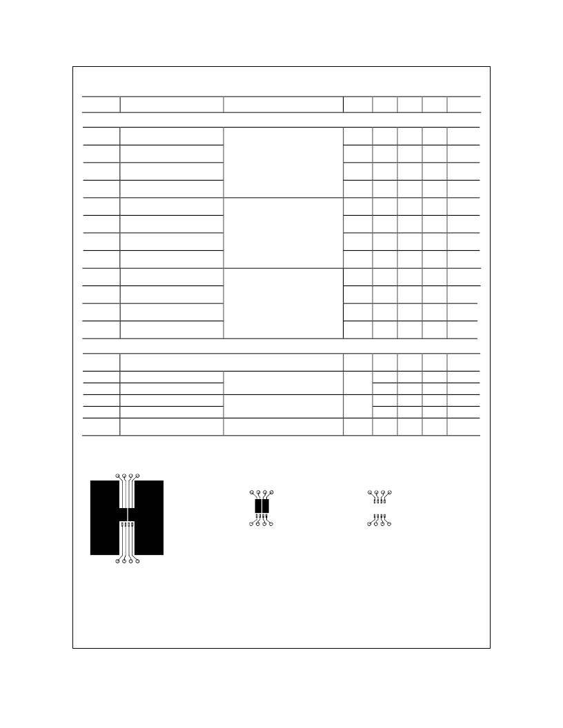
Scale 1 : 1 on letter size paper
2.
See “SyncFET Schottky body diode characteristics” below.
3.
Pulse Test: Pulse Width < 300
μ
s, Duty Cycle < 2.0%
4.
FDS6984AS_NL is a lead free product. The FDS6984AS_NL marking will appear on the reel label.
F
相關PDF資料 |
PDF描述 |
|---|---|
| FDS6984S | Dual Notebook Power Supply N-Channel PowerTrench SyncFET⑩ |
| FDS6984SQ1 | Dual Notebook Power Supply N-Channel PowerTrench SyncFET⑩ |
| FDS6986AS | Dual Notebook Power Supply N-Channel PowerTrench SyncFET |
| FDS6986S | Dual Notebook Power Supply N-Channel PowerTrench SyncFET⑩ |
| FDS6990S | Dual 30V N-Channel PowerTrench SyncFET |
相關代理商/技術參數 |
參數描述 |
|---|---|
| FDS6984AS_08 | 制造商:FAIRCHILD 制造商全稱:Fairchild Semiconductor 功能描述:Dual Notebook Power Supply N-Channel PowerTrench SyncFET |
| FDS6984AS_NL | 制造商:FAIRCHILD 制造商全稱:Fairchild Semiconductor 功能描述:Dual Notebook Power Supply N-Channel PowerTrench SyncFET |
| FDS6984S | 功能描述:MOSFET SO-8 DUAL N-CH RoHS:否 制造商:STMicroelectronics 晶體管極性:N-Channel 汲極/源極擊穿電壓:650 V 閘/源擊穿電壓:25 V 漏極連續電流:130 A 電阻汲極/源極 RDS(導通):0.014 Ohms 配置:Single 最大工作溫度: 安裝風格:Through Hole 封裝 / 箱體:Max247 封裝:Tube |
| FDS6984S | 制造商:Fairchild Semiconductor Corporation 功能描述:MOSFET DUAL NN SO-8 |
| FDS6984S_Q | 功能描述:MOSFET SO-8 DUAL N-CH RoHS:否 制造商:STMicroelectronics 晶體管極性:N-Channel 汲極/源極擊穿電壓:650 V 閘/源擊穿電壓:25 V 漏極連續電流:130 A 電阻汲極/源極 RDS(導通):0.014 Ohms 配置:Single 最大工作溫度: 安裝風格:Through Hole 封裝 / 箱體:Max247 封裝:Tube |
發布緊急采購,3分鐘左右您將得到回復。