- 您現在的位置:買賣IC網 > PDF目錄375831 > FLL1200IU-2 (FUJITSU LTD) L-Band Medium & High Power GaAs FET PDF資料下載
參數資料
| 型號: | FLL1200IU-2 |
| 廠商: | FUJITSU LTD |
| 元件分類: | 功率晶體管 |
| 英文描述: | L-Band Medium & High Power GaAs FET |
| 中文描述: | L BAND, GaAs, N-CHANNEL, RF POWER, JFET |
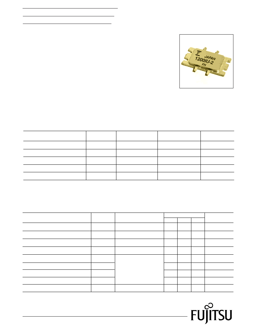
| 封裝: | CASE IU, 6 PIN |
| 文件頁數: | 1/4頁 |
| 文件大小: | 92K |
| 代理商: | FLL1200IU-2 |
1
Edition 1.7
December 1999
FLL1200IU-2
L-Band Medium & High Power GaAs FET
DESCRIPTION
The FLL1200IU-2 is a 120 Watt GaAs FET that employs a push-pull design that
offers ease of matching, greater consistency and a broader bandwidth for high
power L-band amplifiers. This product is targeted to reduce the size and
complexity of highly linear, high power base station transmitting amplifiers.
This new product is uniquely suited for use in PCS/PCN base station amplifiers
as it offers high gain, long term reliability and ease of use.
Fujitsu’s stringent Quality Assurance Program assures the highest
reliability and consistent performance.
FEATURES
Push-Pull Configuration
High Power Output: 120W (Typ.)
High PAE: 44%.
Broad Frequency Range: 1800 to 2000 MHz.
Suitable for class AB operation.
Parameter
Drain-Source Voltage
Gate-Source Voltage
Total Power Dissipation
Storage Temperature
Channel Temperature
Symbol
V
DS
V
GS
P
T
T
stg
Tc = 25
°
C
V
V
W
°
C
°
C
T
ch
Condition
187.5
-65 to +175
+175
-5
15
Rating
Unit
ABSOLUTE MAXIMUM RATINGS (Ambient Temperature Ta=25
°
C)
Fujitsu recommends the following conditions for the reliable operation of GaAs FETs:
1. The drain-source operating voltage (VDS) should not exceed 12 volts.
2. The forward and reverse gate currents should not exceed 156.0 and -57.6 mA respectively with
gate resistance of 10
.
3. The operating channel temperature (Tch) should not exceed 145
°
C.
Item
Drain Current
Transconductance
Pinch-Off Voltage
Gate-Source Breakdown Voltage
Output Power
Linear Gain
Power-Added Efficiency
Thermal Resistance
CASE STYLE: IU
Symbol
I
DSS
V
GSO
-
24
-
-
48
72
-1.0
-2.0
-3.5
-5
-
-
49.8
50.8
-
10.0
11.0
-
-
44
-
-
0.6
0.8
V
DS
= 5V, V
GS
= 0V
V
DS
= 5V, I
DS
= 28.8A
V
DS
= 5V, I
DS
= 2.88A
I
GS
= -2.88mA
Channel to Case
V
DS
= 12V
f=1.96 GHz
I
DS
= 5.0A
Pin = 41.0dBm
A
S
V
dB
dBm
V
°
C/W
%
gm
V
p
P
out
GL
η
add
Drain Current
-
20
30
A
I
DSR
R
th
Conditions
Unit
Limits
Typ.
Max.
Min.
ELECTRICAL CHARACTERISTICS (Ambient Temperature Ta=25
°
C)
相關PDF資料 |
PDF描述 |
|---|---|
| FLL177 | L-BAND MEDIUM & HIGH POWER GAAS FET |
| FLL177ME | L-BAND MEDIUM & HIGH POWER GAAS FET |
| FLL21E180IU | High Voltage - High Power GaAs FET |
| FLL2400IU-2C | L-Band High Power GaAs FET |
| FLL351ME | L-band medium & high power gaas FTEs |
相關代理商/技術參數 |
參數描述 |
|---|---|
| FLL1200IU-3 | 制造商:EUDYNA 制造商全稱:Eudyna Devices Inc 功能描述:L-Band High Power GaAs FET |
| FLL120MK | 制造商:SUMITOMO ELECTRIC Device Innovations Inc 功能描述:Single-end,L-Band, 10dB, 2.3GHz, 2200mA, Bulk |
| FLL1500IU-2C | 制造商:未知廠家 制造商全稱:未知廠家 功能描述:L-Band High Power GaAs FET |
| FLL177 | 制造商:FUJITSU 制造商全稱:Fujitsu Component Limited. 功能描述:L-BAND MEDIUM & HIGH POWER GAAS FET |
| FLL177ME | 制造商:FUJITSU 制造商全稱:Fujitsu Component Limited. 功能描述:L-BAND MEDIUM & HIGH POWER GAAS FET |
發布緊急采購,3分鐘左右您將得到回復。