- 您現(xiàn)在的位置:買賣IC網(wǎng) > PDF目錄375849 > FM3204-S (Electronic Theatre Controls, Inc.) Integrated Processor Companion with Memory PDF資料下載
參數(shù)資料
| 型號: | FM3204-S |
| 廠商: | Electronic Theatre Controls, Inc. |
| 英文描述: | Integrated Processor Companion with Memory |
| 中文描述: | 綜合處理器與記憶體伴侶 |
| 文件頁數(shù): | 12/20頁 |
| 文件大小: | 285K |
| 代理商: | FM3204-S |
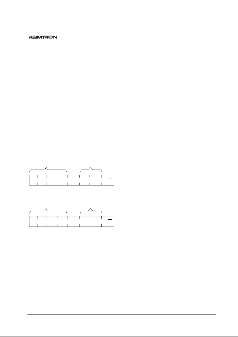
Slave Address
The first byte that the FM32xx expects after a Start
condition is the slave address. As shown in figures
below, the slave address contains the Slave ID,
Device Select address, and a bit that specifies if the
transaction is a read or a write.
The FM32xx has two Slave Addresses (Slave IDs)
associated with two logical devices. To access the
memory device, bits 7-4 should be set to 1010b. The
other logical device within the FM32xx is the real-
time clock and companion. To access this device,
bits 7-4 of the slave address should be set to 1101b.
A bus transaction with this slave address will not
affect the memory in any way. The figures below
illustrate the two Slave Addresses.
The Device Select bits allow multiple devices of the
same type to reside on the 2-wire bus. The device
select bits (bits 2-1) select one of four parts on a two-
wire bus. They must match the corresponding value
on the external address pins in order to select the
device. Bit 0 is the read/write bit. A “1” indicates a
read operation, and a “0” indicates a write operation.
FM3204/16/64/256
Rev 2.1
Dec. 2004
Page 12 of 20
1
0
1
0
X
A1
A0
R/W
Slave ID
Device
Select
7
6
5
4
3
2
1
0
Figure 8. Slave Address - Memory
Figure 9. Slave Address – Companion
Addressing Overview – Memory
After the FM32xx acknowledges the Slave Address,
the master can place the memory address on the bus
for a write operation. The address requires two bytes.
This is true for all members of the family. Therefore
the 4Kb and 16Kb configurations will be addressed
differently from stand alone serial memories but the
entire family will be upwardly compatible with no
software changes.
The first is the MSB (upper byte). For a given
density unused address bits are don’t cares, but
should be set to 0 to maintain upward compatibility.
Following the MSB is the LSB (lower byte) which
contains the remaining eight address bits. The
address is latched internally. Each access causes the
latched address to be incremented automatically. The
current address is the value that is held in the latch,
either a newly written value or the address following
the last access. The current address will be held as
long as V
DD
> V
TP
or until a new value is written.
Accesses to the clock do not affect the current
memory address. Reads always use the current
address. A random read address can be loaded by
beginning a write operation as explained below.
After transmission of each data byte, just prior to the
Acknowledge, the FM32xx increments the internal
address. This allows the next sequential byte to be
accessed with no additional addressing externally.
After the last address is reached, the address latch
will roll over to 0000h. There is no limit to the
number of bytes that can be accessed with a single
read or write operation.
Addressing Overview – Companion
The Processor Companion operate in a similar
manner to the memory, except that it uses only one
byte of address. Addresses 00h to 18h correspond to
special function registers. Attempting to load
addresses above 18h is an illegal condition; the
FM32xx will return a NACK and abort the 2-wire
transaction.
Data Transfer
After the address information has been transmitted,
data transfer between the bus master and the
FM32xx begins. For a read, the FM32xx will place 8
data bits on the bus then wait for an ACK from the
master. If the ACK occurs, the FM32xx will transfer
the next byte. If the ACK is not sent, the FM32xx
will end the read operation. For a write operation, the
FM32xx will accept 8 data bits from the master then
send an Acknowledge. All data transfer occurs MSB
(most significant bit) first.
Memory Write Operation
All memory writes begin with a Slave Address, then
a memory address. The bus master indicates a write
operation by setting the slave address LSB to a 0.
After addressing, the bus master sends each byte of
data to the memory and the memory generates an
Acknowledge condition. Any number of sequential
bytes may be written. If the end of the address range
is reached internally, the address counter will wrap
to 0000h. Internally, the actual memory write occurs
after the 8
th
data bit is transferred. It will be complete
before the Acknowledge is sent. Therefore, if the
user desires to abort a write without altering the
memory contents, this should be done using a Start
1
1
0
1
X
A1
A0
R/W
Slave ID
7
6
5
4
3
2
1
0
Device
Select
相關(guān)PDF資料 |
PDF描述 |
|---|---|
| FM3216 | Integrated Processor Companion with Memory |
| FM3216-G | Integrated Processor Companion with Memory |
| FM3216-S | Integrated Processor Companion with Memory |
| FM32256 | Integrated Processor Companion with Memory |
| FM32256-G | Integrated Processor Companion with Memory |
相關(guān)代理商/技術(shù)參數(shù) |
參數(shù)描述 |
|---|---|
| FM3204-STR | 功能描述:監(jiān)控電路 4K w/Pwr Mon WDT Bat Sw Pwr Fail RoHS:否 制造商:STMicroelectronics 監(jiān)測電壓數(shù): 監(jiān)測電壓: 欠電壓閾值: 過電壓閾值: 輸出類型:Active Low, Open Drain 人工復(fù)位:Resettable 監(jiān)視器:No Watchdog 電池備用開關(guān):No Backup 上電復(fù)位延遲(典型值):10 s 電源電壓-最大:5.5 V 最大工作溫度:+ 85 C 安裝風格:SMD/SMT 封裝 / 箱體:UDFN-6 封裝:Reel |
| FM320A | 制造商:RECTRON 制造商全稱:Rectron Semiconductor 功能描述:SURFACE MOUNT SCHOTTKY BARRIER RECTIFIER VOLTAGE RANGE 20 to 60 Volts CURRENT 3.0 Amperes |
| FM320-A | 制造商:FORMOSA 制造商全稱:Formosa MS 功能描述:Chip Schottky Barrier Diodes - Silicon epitaxial planer type |
| FM320-AL | 制造商:FORMOSA 制造商全稱:Formosa MS 功能描述:Chip Schottky Barrier Diodes - Silicon epitaxial planer type |
| FM320-ALN | 制造商:FORMOSA 制造商全稱:Formosa MS 功能描述:Chip Schottky Barrier Diodes - Silicon epitaxial planer type |
發(fā)布緊急采購,3分鐘左右您將得到回復(fù)。