- 您現在的位置:買賣IC網 > PDF目錄375849 > FM3204-S (Electronic Theatre Controls, Inc.) Integrated Processor Companion with Memory PDF資料下載
參數資料
| 型號: | FM3204-S |
| 廠商: | Electronic Theatre Controls, Inc. |
| 英文描述: | Integrated Processor Companion with Memory |
| 中文描述: | 綜合處理器與記憶體伴侶 |
| 文件頁數: | 16/20頁 |
| 文件大小: | 285K |
| 代理商: | FM3204-S |
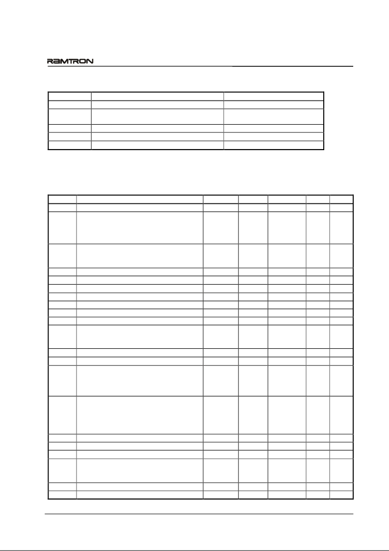
Electrical Specifications
Absolute Maximum Ratings
Symbol
V
DD
V
IN
FM3204/16/64/256
Rev 2.1
Dec. 2004
Page 16 of 20
Description
Ratings
-1.0V to +7.0V
-1.0V to +7.0V * and
V
IN
≤
V
DD
+1.0V **
-1.0V to +4.5V
-55
°
C to + 125
°
C
300
°
C
Power Supply Voltage with respect to V
SS
Voltage on any signal pin with respect to V
SS
V
BAK
T
STG
T
LEAD
Backup Supply Voltage
Storage Temperature
Lead Temperature (Soldering, 10 seconds)
* PFI input voltage must not exceed 4.5V.
** The “V
IN
< V
DD
+1.0V” restriction does not apply to the SCL and SDA inputs which do not employ a diode to V
DD
.
Stresses above those listed under Absolute Maximum Ratings may cause permanent damage to the device. This is a stress rating
only, and the functional operation of the device at these or any other conditions above those listed in the operational section of this
specification is not implied. Exposure to absolute maximum ratings conditions for extended periods may affect device reliability.
DC Operating Conditions
(
T
A
= -40
°
C to + 85
°
C, V
DD
= 2.7V to 5.5V unless otherwise specified)
Symbol
Parameter
V
DD
Main Power Supply
I
DD
V
DD
Supply Current
@ SCL = 100 kHz
@ SCL = 400 kHz
@ SCL = 1 MHz
I
SB
Standby Current
For V
DD
< 5.5V
For V
DD
< 3.6V
V
BAK
Backup Supply Voltage
I
BAK
Backup Supply Current
I
BAKTC
Trickle Charge Current
V
TP0
V
DD
Trip Point Voltage, VTP(1:0) = 00b
V
TP1
V
DD
Trip Point Voltage, VTP(1:0) = 01b
V
TP2
V
DD
Trip Point Voltage, VTP(1:0) = 10b
V
TP3
V
DD
Trip Point Voltage, VTP(1:0) = 11b
V
RST
V
DD
for valid /RST @ I
OL
= 80
μ
A at V
OL
V
BAK
> V
BAK
min
V
BAK
< V
BAK
min
I
LI
Input Leakage Current
I
LO
Output Leakage Current
V
IL
Input Low Voltage
All inputs except those listed below
CNT1-2 battery backed (V
DD
< 2.5V)
CNT1-2 (V
DD
> 2.5V)
V
IH
Input High Voltage
All inputs except those listed below
PFI (comparator input)
CNT1-2 battery backed (V
DD
< 2.5V)
CNT1-2 V
DD
> 2.5V
V
OL
Output Low Voltage (I
OL
= 3 mA)
V
OH
Output High Voltage (I
OH
= -2 mA)
R
RST
Pull-up resistance for /RST inactive
R
IN
Input Resistance (pulldown)
A1-A0 for V
IN
= V
IL
max
A1-A0 for V
IN
= V
IH
min
V
PFI
Power Fail Input Reference Voltage
V
HYS
Power Fail Input (PFI) Hysteresis (Rising)
Min
2.7
Typ
Max
5.5
500
900
1500
150
120
3.75
1
25
2.70
3.00
4.00
4.50
Units
V
μ
A
μ
A
μ
A
μ
A
μ
A
V
μ
A
μ
A
V
V
V
V
V
V
μ
A
μ
A
V
V
V
V
V
V
V
V
V
K
K
M
V
mV
Notes
7
1
2
2.0
5
2.55
2.85
3.80
4.25
0
1.6
-0.3
-0.3
-0.3
0.7 V
DD
-
V
BAK
– 0.5
0.7 V
DD
-
2.4
50
20
1
1.175
3.0
2.6
2.9
3.9
4.4
9
4
10
5
5
5
5
6
1
1
3
3
8
0.3 V
DD
0.5
0.8
V
DD
+ 0.3
3.75
V
BAK
+ 0.3
V
DD
+ 0.3
0.4
-
400
1.20
-
1.225
100
相關PDF資料 |
PDF描述 |
|---|---|
| FM3216 | Integrated Processor Companion with Memory |
| FM3216-G | Integrated Processor Companion with Memory |
| FM3216-S | Integrated Processor Companion with Memory |
| FM32256 | Integrated Processor Companion with Memory |
| FM32256-G | Integrated Processor Companion with Memory |
相關代理商/技術參數 |
參數描述 |
|---|---|
| FM3204-STR | 功能描述:監控電路 4K w/Pwr Mon WDT Bat Sw Pwr Fail RoHS:否 制造商:STMicroelectronics 監測電壓數: 監測電壓: 欠電壓閾值: 過電壓閾值: 輸出類型:Active Low, Open Drain 人工復位:Resettable 監視器:No Watchdog 電池備用開關:No Backup 上電復位延遲(典型值):10 s 電源電壓-最大:5.5 V 最大工作溫度:+ 85 C 安裝風格:SMD/SMT 封裝 / 箱體:UDFN-6 封裝:Reel |
| FM320A | 制造商:RECTRON 制造商全稱:Rectron Semiconductor 功能描述:SURFACE MOUNT SCHOTTKY BARRIER RECTIFIER VOLTAGE RANGE 20 to 60 Volts CURRENT 3.0 Amperes |
| FM320-A | 制造商:FORMOSA 制造商全稱:Formosa MS 功能描述:Chip Schottky Barrier Diodes - Silicon epitaxial planer type |
| FM320-AL | 制造商:FORMOSA 制造商全稱:Formosa MS 功能描述:Chip Schottky Barrier Diodes - Silicon epitaxial planer type |
| FM320-ALN | 制造商:FORMOSA 制造商全稱:Formosa MS 功能描述:Chip Schottky Barrier Diodes - Silicon epitaxial planer type |
發布緊急采購,3分鐘左右您將得到回復。