- 您現在的位置:買賣IC網 > PDF目錄375864 > FMS6501 (Fairchild Semiconductor Corporation) 12 Input 9 Output Video Switch Matrix with Input Clamp, Input Bias Circuitry, and Output Drivers PDF資料下載
參數資料
| 型號: | FMS6501 |
| 廠商: | Fairchild Semiconductor Corporation |
| 英文描述: | 12 Input 9 Output Video Switch Matrix with Input Clamp, Input Bias Circuitry, and Output Drivers |
| 中文描述: | 12輸入9輸出與輸入鉗位,偏置電路的輸入和輸出視頻開關矩陣驅動 |
| 文件頁數: | 8/16頁 |
| 文件大小: | 166K |
| 代理商: | FMS6501 |
8
www.fairchildsemi.com
FMS6501 Rev. 1A
F
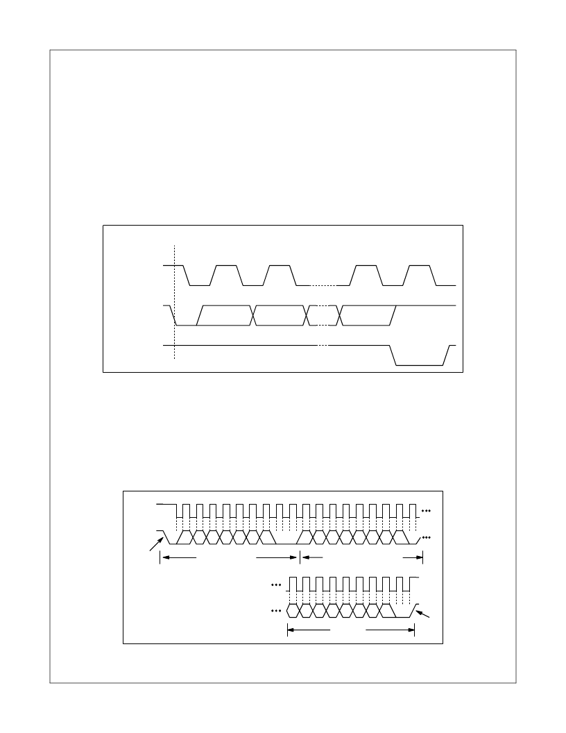
Figure 4: Acknowledgement on the I
2
C Bus
Acknowledge
The number of data bytes transferred between the start
and stop conditions from transmitter to receiver is unlim-
ited. Each byte of eight bits is followed by an acknowl-
edge bit. The acknowledge bit is a HIGH level signal put
on the bus by the transmitter during which time the mas-
ter generates an extra acknowledge related clock pulse.
A slave receiver which is addressed must generate an
acknowledge after the reception of each byte. Also a
master receiver must generate an acknowledge after the
reception of each byte that has been clocked out of the
slave transmitter.
The device that acknowledges must pull down the SDA
line during the acknowledge clock pulse, so that the SDA
line is stable LOW during the HIGH period of the acknowl-
edge related clock pulse (set-up and hold times must be
taken into consideration). A master receiver must signal
an end of data to the transmitter by not generating an
acknowledge on the last byte that has been clocked out
of the slave. In this event the transmitter must leave the
data line HIGH to enable the master to generate a stop
condition.
SCL FROM
MASTER
DATA OUTPUT
BY TRANSMITTER
DATA OUTPUT
BY RECEIVER
START
condition
1
2
8
9
clock pulse for
acknowledgement
I
2
C Bus Protocol
Before any data is transmitted on the I
2
C bus, the device which should respond is addressed first. The addressing is always
carried out with the first byte transmitted after the start procedure. The I
2
C bus configuration for a data write to the FMS6501 is
shown below in figure 5:
Figure 5: Write a register address to the pointer register, then write data to the selected register
A6
A5
A4
A3
A2
A1
A0
1
9
R/W
D7
D6
D5
D4
D3
D2
D1
D0
07
1
9
ACK. BY
FMS6501
ACK. BY
FMS6501
FRAME1
SERIAL BUS ADDRESS BYTE
ADDRESS POFRAME 2
1
9
D7
D6
D5
D4
D3
D2
D1
D0
ACK. BY
FMS6501
FRAME 3
DATA BYTE
SCL
SDA
START BY
STOP BY
SCL(CONTINUED)
SDA(CONTINUED)
相關PDF資料 |
PDF描述 |
|---|---|
| FMS6501MSA28 | 12 Input 9 Output Video Switch Matrix with Input Clamp, Input Bias Circuitry, and Output Drivers |
| FMS6501MSA28X | 12 Input 9 Output Video Switch Matrix with Input Clamp, Input Bias Circuitry, and Output Drivers |
| FMS6690 | Six Channel, 6th Order SD/PS/HD Video Filter Driver |
| FMS6690MTC20X | Six Channel, 6th Order SD/PS/HD Video Filter Driver |
| FMS6G10US60S | Compact & Complex Module |
相關代理商/技術參數 |
參數描述 |
|---|---|
| FMS6501_06 | 制造商:FAIRCHILD 制造商全稱:Fairchild Semiconductor 功能描述:12 Input / 9 Output Video Switch Matrix with Input Clamp, Input Bias Circuitry, and Output Drivers |
| FMS6501_07 | 制造商:FAIRCHILD 制造商全稱:Fairchild Semiconductor 功能描述:12 Input / 9 Output Video Switch Matrix with Input Clamp, Input Bias Circuitry, and Output Drivers |
| FMS6501AMTC28X | 功能描述:視頻 IC 12 Input, 9 Output Video Switch Matrix RoHS:否 制造商:Fairchild Semiconductor 工作電源電壓:5 V 電源電流:80 mA 最大工作溫度:+ 85 C 封裝 / 箱體:TSSOP-28 封裝:Reel |
| FMS6501MSA28 | 功能描述:視頻 IC 12 Input 9 Output VideoSwtch RoHS:否 制造商:Fairchild Semiconductor 工作電源電壓:5 V 電源電流:80 mA 最大工作溫度:+ 85 C 封裝 / 箱體:TSSOP-28 封裝:Reel |
| FMS6501MSA28X | 功能描述:視頻 IC 12 Input 9 Output VideoSwtch RoHS:否 制造商:Fairchild Semiconductor 工作電源電壓:5 V 電源電流:80 mA 最大工作溫度:+ 85 C 封裝 / 箱體:TSSOP-28 封裝:Reel |
發布緊急采購,3分鐘左右您將得到回復。