- 您現在的位置:買賣IC網 > PDF目錄385320 > GS8322V36GE-166 (GSI TECHNOLOGY) 2M x 18, 1M x 36, 512K x 72 36Mb S/DCD Sync Burst SRAMs PDF資料下載
參數資料
| 型號: | GS8322V36GE-166 |
| 廠商: | GSI TECHNOLOGY |
| 元件分類: | DRAM |
| 英文描述: | 2M x 18, 1M x 36, 512K x 72 36Mb S/DCD Sync Burst SRAMs |
| 中文描述: | 1M X 36 CACHE SRAM, 8 ns, PBGA165 |
| 封裝: | 15 X 17 MM, 1 MM PITCH, LEAD FREE, FPBGA-165 |
| 文件頁數: | 30/42頁 |
| 文件大小: | 1038K |
| 代理商: | GS8322V36GE-166 |
第1頁第2頁第3頁第4頁第5頁第6頁第7頁第8頁第9頁第10頁第11頁第12頁第13頁第14頁第15頁第16頁第17頁第18頁第19頁第20頁第21頁第22頁第23頁第24頁第25頁第26頁第27頁第28頁第29頁當前第30頁第31頁第32頁第33頁第34頁第35頁第36頁第37頁第38頁第39頁第40頁第41頁第42頁
Select DR
Capture DR
0
Shift DR
Exit1 DR
Pause DR
Exit2 DR
Update DR
1
Select IR
Capture IR
0
Shift IR
Exit1 IR
Pause IR
Exit2 IR
Update IR
1
Test Logic Reset
Run Test Idle
0
1
0
1
1
0
1
1
1
0
0
1
1
0
0
0
0
1
1
0
0
0
0
0
1
1
1
1
Preliminary
GS8322V18(B/E)/GS8322V36(B/E)/GS8322V72(C)
Specifications cited are subject to change without notice. For latest documentation see http://www.gsitechnology.com.
Rev: 1.04 4/2005
30/42
2003, GSI Technology
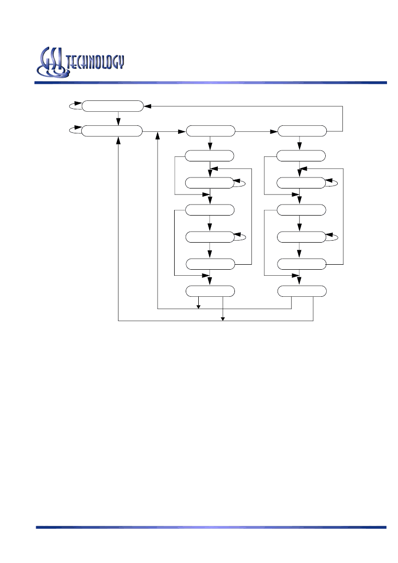
JTAG Tap Controller State Diagram
Instruction Descriptions
BYPASS
When the BYPASS instruction is loaded in the Instruction Register the Bypass Register is placed between TDI and TDO. This
occurs when the TAP controller is moved to the Shift-DR state. This allows the board level scan path to be shortened to facili-
tate testing of other devices in the scan path.
SAMPLE/PRELOAD
SAMPLE/PRELOAD is a Standard 1149.1 mandatory public instruction. When the SAMPLE / PRELOAD instruction is
loaded in the Instruction Register, moving the TAP controller into the Capture-DR state loads the data in the RAMs input and
I/O buffers into the Boundary Scan Register. Boundary Scan Register locations are not associated with an input or I/O pin, and
are loaded with the default state identified in the Boundary Scan Chain table at the end of this section of the datasheet. Because
the RAM clock is independent from the TAP Clock (TCK) it is possible for the TAP to attempt to capture the I/O ring contents
while the input buffers are in transition (i.e. in a metastable state). Although allowing the TAP to sample metastable inputs will
not harm the device, repeatable results cannot be expected. RAM input signals must be stabilized for long enough to meet the
TAPs input data capture set-up plus hold time (tTS plus tTH). The RAMs clock inputs need not be paused for any other TAP
operation except capturing the I/O ring contents into the Boundary Scan Register. Moving the controller to Shift-DR state then
places the boundary scan register between the TDI and TDO pins.
EXTEST
EXTEST is an IEEE 1149.1 mandatory public instruction. It is to be executed whenever the instruction register is loaded with
all logic 0s. The EXTEST command does not block or override the RAM’s input pins; therefore, the RAM’s internal state is
still determined by its input pins.
相關PDF資料 |
PDF描述 |
|---|---|
| GS8322V36GE-166I | 2M x 18, 1M x 36, 512K x 72 36Mb S/DCD Sync Burst SRAMs |
| GS8322V36GE-200 | 2M x 18, 1M x 36, 512K x 72 36Mb S/DCD Sync Burst SRAMs |
| GS8322V36GE-200I | 2M x 18, 1M x 36, 512K x 72 36Mb S/DCD Sync Burst SRAMs |
| GS8322V36GE-225 | 2M x 18, 1M x 36, 512K x 72 36Mb S/DCD Sync Burst SRAMs |
| GS8322V36GE-225I | 2M x 18, 1M x 36, 512K x 72 36Mb S/DCD Sync Burst SRAMs |
相關代理商/技術參數 |
參數描述 |
|---|---|
| GS8322V72C-133 | 制造商:GSI Technology 功能描述:SRAM SYNC OCTAL 1.8V 36MBIT 512KX72 8.5NS/4NS 209FBGA - Trays |
| GS8322V72C-133I | 制造商:GSI Technology 功能描述:SRAM SYNC OCTAL 1.8V 36MBIT 512KX72 8.5NS/4NS 209FBGA - Trays |
| GS8322V72C-150 | 制造商:GSI Technology 功能描述:SRAM SYNC OCTAL 1.8V 36MBIT 512KX72 8.5NS/3.8NS 209FBGA - Trays |
| GS8322V72C-150I | 制造商:GSI Technology 功能描述:SRAM SYNC OCTAL 1.8V 36MBIT 512KX72 8.5NS/3.8NS 209FBGA - Trays |
| GS8322V72C-166 | 制造商:GSI Technology 功能描述:SRAM SYNC OCTAL 1.8V 36MBIT 512KX72 8NS/3.5NS 209FBGA - Trays |
發布緊急采購,3分鐘左右您將得到回復。