- 您現(xiàn)在的位置:買(mǎi)賣(mài)IC網(wǎng) > PDF目錄385338 > GS8662S09E-200I (GSI TECHNOLOGY) 72Mb Burst of 2 DDR SigmaSIO-II SRAM PDF資料下載
參數(shù)資料
| 型號(hào): | GS8662S09E-200I |
| 廠商: | GSI TECHNOLOGY |
| 元件分類(lèi): | DRAM |
| 英文描述: | 72Mb Burst of 2 DDR SigmaSIO-II SRAM |
| 中文描述: | 8M X 9 DDR SRAM, 0.45 ns, PBGA165 |
| 封裝: | 15 X 17 MM, 1 MM PITCH, MO-216CAB-1, FPBGA-165 |
| 文件頁(yè)數(shù): | 28/37頁(yè) |
| 文件大小: | 960K |
| 代理商: | GS8662S09E-200I |
第1頁(yè)第2頁(yè)第3頁(yè)第4頁(yè)第5頁(yè)第6頁(yè)第7頁(yè)第8頁(yè)第9頁(yè)第10頁(yè)第11頁(yè)第12頁(yè)第13頁(yè)第14頁(yè)第15頁(yè)第16頁(yè)第17頁(yè)第18頁(yè)第19頁(yè)第20頁(yè)第21頁(yè)第22頁(yè)第23頁(yè)第24頁(yè)第25頁(yè)第26頁(yè)第27頁(yè)當(dāng)前第28頁(yè)第29頁(yè)第30頁(yè)第31頁(yè)第32頁(yè)第33頁(yè)第34頁(yè)第35頁(yè)第36頁(yè)第37頁(yè)
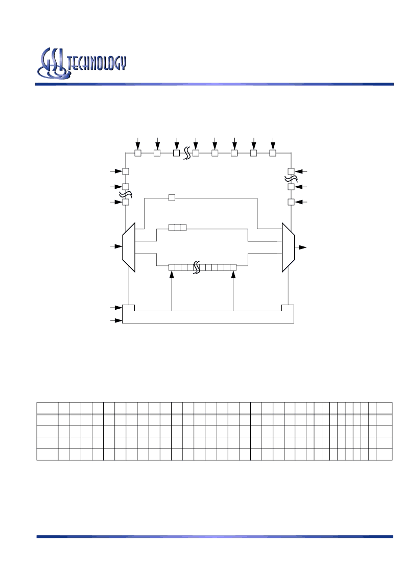
Instruction Register
ID Code Register
·
31 30 29
Boundary Scan Register
0
1
2
0
· · ·
1
2
0
Bypass Register
TDI
TDO
TMS
TCK
Test Access Port (TAP) Controller
1
·
1
0
·
·
·
·
·
·
·
·
·
Control Signals
·
Preliminary
GS8662S08/09/18/36E-333/300/250/200/167
Specifications cited are subject to change without notice. For latest documentation see http://www.gsitechnology.com.
Rev: 1.01 9/2005
28/37
2005, GSI Technology
JTAG TAP Block Diagram
Identification (ID) Register
The ID Register is a 32-bit register that is loaded with a device and vendor specific 32-bit code when the controller is put in
Capture-DR state with the IDCODE command loaded in the Instruction Register. The code is loaded from a 32-bit on-chip ROM.
It describes various attributes of the RAM as indicated below. The register is then placed between the TDI and TDO pins when the
controller is moved into Shift-DR state. Bit 0 in the register is the LSB and the first to reach TDO when shifting begins.
ID Register Contents
Bit #
31 30 29 28 27 26 25 24 23 22 21 20 19 18 17 16 15 14 13 12 11 10 9 8 7 6 5 4 3 2 1
0
x36
X
X
X
X
0
0
0
0
1
0
0
0
1
0
0
1
0
0
0
0
0
0
0 1 1 0 1 1 0 0 1
1
x18
X
X
X
X
0
0
0
0
1
0
0
0
1
0
0
1
0
0
1
0
0
0
0 1 1 0 1 1 0 0 1
1
x9
X
X
X
X
0
0
0
0
1
0
0
0
1
0
0
1
0
0
1
1
0
0
0 1 1 0 1 1 0 0 1
1
x8
X
X
X
X
0
0
0
0
1
0
0
0
1
0
0
1
0
1
1
1
0
0
0 1 1 0 1 1 0 0 1
1
Tap Controller Instruction Set
Overview
There are two classes of instructions defined in the Standard 1149.1-1990; the standard (Public) instructions, and device specific
(Private) instructions. Some Public instructions are mandatory for 1149.1 compliance. Optional Public instructions must be
implemented in prescribed ways. The TAP on this device may be used to monitor all input and I/O pads, and can be used to load
address, data or control signals into the RAM or to preload the I/O buffers.
相關(guān)PDF資料 |
PDF描述 |
|---|---|
| GS8662S09E-250 | 72Mb Burst of 2 DDR SigmaSIO-II SRAM |
| GS88136AD-133 | 512K x 18, 256K x 36 9Mb Synchronous Burst SRAMs |
| GS88136AT-150 | 512K x 18, 256K x 36 9Mb Synchronous Burst SRAMs |
| GS88136AT-150I | 512K x 18, 256K x 36 9Mb Synchronous Burst SRAMs |
| GS88136AT-166 | 512K x 18, 256K x 36 9Mb Synchronous Burst SRAMs |
相關(guān)代理商/技術(shù)參數(shù) |
參數(shù)描述 |
|---|---|
| GS8662S09E-250 | 制造商:GSI 制造商全稱(chēng):GSI Technology 功能描述:72Mb Burst of 2 DDR SigmaSIO-II SRAM |
| GS8662S09E-250I | 制造商:GSI 制造商全稱(chēng):GSI Technology 功能描述:72Mb Burst of 2 DDR SigmaSIO-II SRAM |
| GS8662S09E-300 | 制造商:GSI 制造商全稱(chēng):GSI Technology 功能描述:72Mb Burst of 2 DDR SigmaSIO-II SRAM |
| GS8662S09E-300I | 制造商:GSI 制造商全稱(chēng):GSI Technology 功能描述:72Mb Burst of 2 DDR SigmaSIO-II SRAM |
| GS8662S09E-333 | 制造商:GSI 制造商全稱(chēng):GSI Technology 功能描述:72Mb Burst of 2 DDR SigmaSIO-II SRAM |
發(fā)布緊急采購(gòu),3分鐘左右您將得到回復(fù)。