- 您現在的位置:買賣IC網 > PDF目錄385353 > HA457 (Intersil Corporation) 95MHz, Low Power, AV = 2, 8 x 8 Video Crosspoint Switch PDF資料下載
參數資料
| 型號: | HA457 |
| 廠商: | Intersil Corporation |
| 英文描述: | 95MHz, Low Power, AV = 2, 8 x 8 Video Crosspoint Switch |
| 中文描述: | 95MHz,低功耗,影音\u003d 2,8 × 8視頻交叉點開關 |
| 文件頁數: | 1/14頁 |
| 文件大小: | 175K |
| 代理商: | HA457 |
1
File Number
4231.2
HA457
95MHz, Low Power, A
V
= 2, 8 x 8 Video
Crosspoint Switch
The HA457 is an 8 x 8 video crosspoint switch suitable for
high performance video systems. Its high level of integration
significantly reduces component count, board space, and
cost. The crosspoint switch contains a digitally controlled
matrix of 64 fully buffered switches that connect eight video
input signals to any, or all, matrix outputs. Each matrix output
connects to an internal, high-speed (275V/
μ
s), gain of two
buffer capable of driving 150
to
±
2.5V.
The HA457 will directly drive a double terminated video
cable with some degradation of differential gain and phase.
Applications demanding the best composite video
performance should drive the cable with a unity gain video
buffer, such as the HFA1412 quad buffer (see Figure 7).
This crosspoint’s three-state output capability makes it
feasible to parallel multiple HA457s and form larger switch
matrices.
Features
Pin Compatible, Cable Driving Upgrade for HA456 and
MAX456
Fully Buffered Inputs and Outputs (A
V
= +2)
Routes Any Input Channel to Any Output Channel
Switches Standard and High Resolution Video Signals
Serial or Parallel Digital Interface
Expandable for Larger Switch Matrices
Wide Bandwidth . . . . . . . . . . . . . . . . . . . . . . . . . . . 95MHz
High Slew Rate. . . . . . . . . . . . . . . . . . . . . . . . . . . 275V/
μ
s
Low Crosstalk at 10MHz . . . . . . . . . . . . . . . . . . . . -55dB
Applications
Video Switching and Routing
Security and Video Editing Systems
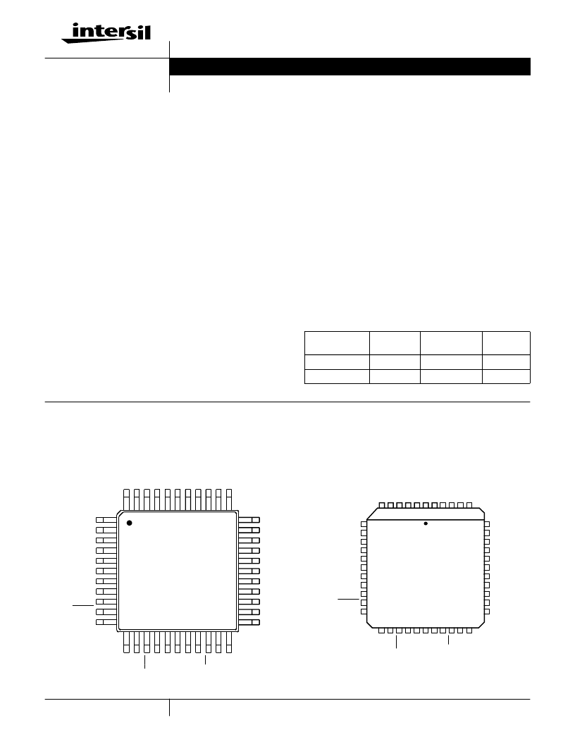
Pinouts
Ordering Information
PART NUMBER
TEMP.
RANGE (
o
C)
PACKAGE
PKG. NO.
HA457CN
0 to 70
44 Ld MQFP
Q44.10x10
HA457CM
0 to 70
44 Ld PLCC
N44.65
HA457 (MQFP)
TOP VIEW
HA457 (PLCC)
TOP VIEW
1
2
3
4
5
6
7
8
9
10
11
12 13 14 15 16 17
28
27
26
25
24
23
22
21
20
19
18
39 38 37 36 3534
33
32
31
30
29
44 43 42 41 40
I
A
A
D
D
N
V
O
D
O
D
A0
IN1
NC
IN2
DGND
NC
IN3
DGND
IN4
EDGE/LEVEL
IN5
OUT2
V-
OUT3
AGND
OUT4
NC
AGND
OUT5
AGND
OUT6
V+
V
I
S
I
V
N
W
L
C
C
O
44 43 42 41 40
39
38
37
36
35
34
33
32
31
30
29
28
27
1
2
3
4
5
6
26
25
24
23
22
21
20
19
18
7
8
9
10
11
12
13
14
15
16
17
A0
IN1
NC
IN2
DGND
NC
IN3
DGND
IN4
EDGE/LEVEL
IN5
I
A
A
D
D
N
V
O
D
O
D
V
I
S
I
V
N
W
L
C
C
O
OUT2
V-
OUT3
AGND
OUT4
NC
AGND
OUT5
AGND
OUT6
V+
Data Sheet
August 1999
CAUTION: These devices are sensitive to electrostatic discharge; follow proper IC Handling Procedures.
1-888-INTERSIL or 321-724-7143
|
Copyright
Intersil Corporation 1999
相關PDF資料 |
PDF描述 |
|---|---|
| HA4905 | () |
| HA5013 | Triple, 125MHz Video Amplifier |
| HA5013IP | Triple, 125MHz Video Amplifier |
| HA5013IB | Hook-Up Wire; Conductor Size AWG:30; No. Strands x Strand Size:Solid; Jacket Color:Purple; Approval Bodies:UL, CSA; Approval Categories:UL AWM Style 1061; CSA AWM; Conductor Material:Copper; Jacket Material:Polyvinylchloride (PVC) RoHS Compliant: Yes |
| HA5221 | HA-5221/22 SPICE OPERATIONAL AMPLIFIER MACRO-MODEL |
相關代理商/技術參數 |
參數描述 |
|---|---|
| HA457CM | 制造商:Rochester Electronics LLC 功能描述:- Bulk |
| HA457CN | 制造商:Rochester Electronics LLC 功能描述:- Bulk |
| HA-460 | 制造商:未知廠家 制造商全稱:未知廠家 功能描述:CRYSTAL CLOCK OSCILLATORS |
| HA4600 | 制造商:INTERSIL 制造商全稱:Intersil Corporation 功能描述:480MHz, SOT-23, Video Buffer with Output Disable |
| HA4600_05 | 制造商:INTERSIL 制造商全稱:Intersil Corporation 功能描述:480MHz, SOT-23, Video Buffer with Output Disable |
發布緊急采購,3分鐘左右您將得到回復。