- 您現在的位置:買賣IC網 > PDF目錄385353 > HAF70009 (Intersil Corporation) 56A, 100V, 0.025 Ohm, N-Channel UltraFET Power MOSFET PDF資料下載
參數資料
| 型號: | HAF70009 |
| 廠商: | Intersil Corporation |
| 英文描述: | 56A, 100V, 0.025 Ohm, N-Channel UltraFET Power MOSFET |
| 中文描述: | 第56A,100V的,0.025 Ohm的N溝道UltraFET功率MOSFET |
| 文件頁數: | 1/10頁 |
| 文件大小: | 107K |
| 代理商: | HAF70009 |
4-1
File Number
4770
CAUTION: These devices are sensitive to electrostatic discharge; follow proper IC Handling Procedures.
http://www.intersil.com or 407-727-9207 | Copyright Intersil Corporation 1999. SABER
is a Copyright of Analogy, Inc.
UltraFET is a trademark of Intersil Corporation. PSPICE is a registered trademark of MicroSim Corporation.
HAF70009
56A, 100V 0.025 Ohm, N-Channel
UltraFET Power MOSFET
This N-Channel power MOSFET is
manufactured using the innovative
UltraFET process. This advanced
process technology achieves the
lowest possible on-resistance per silicon area, resulting in
outstanding performance. This device is capable of
withstanding high energy in the avalanche mode and the
diode exhibits very low reverse recovery time and stored
charge. It was designed for use in applications where power
efficiency is important, such as switching regulators,
switching converters, motor drivers, relay drivers, low-
voltage bus switches, and power management in portable
and battery-operated products.
Formerly developmental type TA75639.
Features
56A, 100V
Simulation Models
- Temperature Compensated PSPICE
and SABER
Electrical Models
- Spice and Saber Thermal Impedance Models
- www.intersil.com
Peak Current vs Pulse Width Curve
UIS Rating Curve
Related Literature
- TB334, “Guidelines for Soldering Surface Mount
Components to PC Boards”
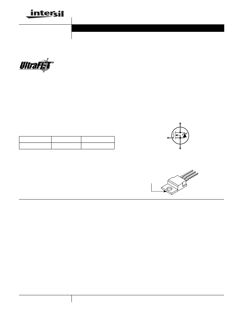
Symbol
Packaging
JEDEC TO-220AB
Ordering Information
PART NUMBER
PACKAGE
TEMP. RANGE (
o
C)
HAF70009
TO-220AB
-55 to 175
D
G
S
GATE
SDRAIN
DRAIN
(FLANGE)
Absolute Maximum Ratings
T
C
= 25
o
C, Unless Otherwise Specified
HAF70009
100
100
±
20
UNITS
V
V
V
Drain to Source Voltage (Note 1). . . . . . . . . . . . . . . . . . . . . . . . . . . . . . . . . . . . . . . . . . . . . . . V
DSS
Drain to Gate Voltage (R
GS
= 20k
) (Note 1) . . . . . . . . . . . . . . . . . . . . . . . . . . . . . . . . . . . . .V
DGR
Gate to Source Voltage . . . . . . . . . . . . . . . . . . . . . . . . . . . . . . . . . . . . . . . . . . . . . . . . . . . . . . . V
GS
Drain Current
Continuous (Figure 2). . . . . . . . . . . . . . . . . . . . . . . . . . . . . . . . . . . . . . . . . . . . . . . . . . . . . . . . .I
D
Pulsed Drain Current . . . . . . . . . . . . . . . . . . . . . . . . . . . . . . . . . . . . . . . . . . . . . . . . . . . . . . . I
DM
Pulsed Avalanche Rating. . . . . . . . . . . . . . . . . . . . . . . . . . . . . . . . . . . . . . . . . . . . . . . . . . . . . . E
AS
Power Dissipation . . . . . . . . . . . . . . . . . . . . . . . . . . . . . . . . . . . . . . . . . . . . . . . . . . . . . . . . . . . . P
D
Derate Above 25
o
C . . . . . . . . . . . . . . . . . . . . . . . . . . . . . . . . . . . . . . . . . . . . . . . . . . . . . . . . . . .
Operating and Storage Temperature . . . . . . . . . . . . . . . . . . . . . . . . . . . . . . . . . . . . . . . . . T
J
, T
STG
Maximum Temperature for Soldering
Leads at 0.063in (1.6mm) from Case for 10s. . . . . . . . . . . . . . . . . . . . . . . . . . . . . . . . . . . . . . T
L
Package Body for 10s, See Tech Brief 334 . . . . . . . . . . . . . . . . . . . . . . . . . . . . . . . . . . . . . .T
pkg
56
Figure 4
A
Figures 6, 14, 15
200
1.35
-55 to 175
W
W/
o
C
o
C
300
260
o
C
o
C
CAUTION: Stresses above those listed in “Absolute Maximum Ratings” may cause permanent damage to the device. This is a stress only rating and operation of the
device at these or any other conditions above those indicated in the operational sections of this specification is not implied.
NOTE:
1. T
J
= 25
o
C to 150
o
C.
Data Sheet
August 1999
相關PDF資料 |
PDF描述 |
|---|---|
| HAT-3 | Precision Fixed Attenuator |
| HBG1105W | Single Color 3216 Dome Lenz Type |
| HBR1105W | Single Color 3216 Dome Lenz Type |
| HBG5066X | Single Color High Brightness ヵ5 Type |
| HBR5066X | Single Color High Brightness ヵ5 Type |
相關代理商/技術參數 |
參數描述 |
|---|---|
| HAF71-2508-05 | 制造商:FW Bell 功能描述:HEAVY DUTY AXIAL PROBE |
| HAF71-2508-05-T | 制造商:FW Bell 功能描述:HEAVY DUTY AXIAL PROBE |
| HA-F71L-NP | 制造商:JVC Worldwide 功能描述:HEADPHONE |
| HA-F71W-NP | 制造商:JVC Worldwide 功能描述:HEADPHONE |
| HA-F75V | 制造商:JVC Worldwide 功能描述:HEADPHONE |
發布緊急采購,3分鐘左右您將得到回復。