- 您現在的位置:買賣IC網 > PDF目錄385382 > HIP6018B (Intersil Corporation) 100,000 System Gate FPGA - NOT RECOMMENDED for NEW DESIGN PDF資料下載
參數資料
| 型號: | HIP6018B |
| 廠商: | Intersil Corporation |
| 英文描述: | 100,000 System Gate FPGA - NOT RECOMMENDED for NEW DESIGN |
| 中文描述: | 先進的雙PWM和線性功率控制 |
| 文件頁數: | 7/14頁 |
| 文件大小: | 134K |
| 代理商: | HIP6018B |
2-244
Description
Operation
The HIP6018B monitors and precisely controls 4 output
voltage levels (Refer to Figures 1, 2, and 3). It is designed for
microprocessor computer applications with 3.3V and 5V
power, and 12V bias input from an ATX power supply. The IC
has one PWM controller, a linear controller, and a linear
regulator. The PWM controller is designed to regulate the
microprocessor core voltage (V
OUT1
) by driving 2 MOSFETs
(Q1 and Q2) in a synchronous-rectified buck converter
configuration. The core voltage is regulated to a level
programmed by the 5-bit digital-to-analog converter (DAC).
An integrated linear regulator supplies the 2.5V clock power
(V
OUT2
). The linear controller drives an external MOSFET
(Q3) to supply the GTL bus power (V
OUT3
).
Initialization
The HIP6018B automatically initializes upon receipt of input
power. Special sequencing of the input supplies is not
necessary. The Power-On Reset (POR) function continually
monitors the input supply voltages. The POR monitors the
bias voltage (+12V
IN
) at the VCC pin, the 5V input voltage
(+5V
IN
) on the OCSET1 pin, and the 3.3V input on the VIN2
pin. The normal level on OCSET1 is equal to +5V
IN
less a
fixed voltage drop (see over-current protection). The POR
function initiates soft-start operation after all three input supply
voltages exceed their POR thresholds.
Soft-Start
The POR function initiates the soft-start sequence. Initially,
the voltage on the SS pin rapidly increases to approximately
1V (this minimizes the soft-start interval). Then an internal
11
μ
A current source charges an external capacitor (C
SS
) on
the SS pin to 4V. The PWM error amplifier reference input
(+terminal) and output (COMP1 pin) is clamped to a level
proportional to the SS pin voltage. As the SS pin voltage
slews from 1V to 4V, the output clamp generates PHASE
pulses of increasing width that charge the output
capacitor(s). After this initial stage, the reference input clamp
slows the output voltage rate-of-rise and provides a smooth
transition to the final set voltage. Additionally both linear
regulator’s reference inputs are clamped to a voltage
proportional to the SS pin voltage. This method provides a
rapid and controlled output voltage rise.
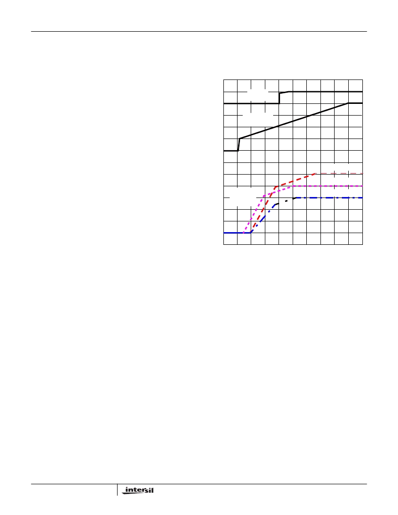
Figure 3 shows the soft-start sequence for the typical
application. At T0 the SS voltage rapidly increases to
approximately 1V. At T1, the SS pin and error amplifier
output voltage reach the valley of the oscillator’s triangle
wave. The oscillator’s triangular waveform is compared to
the clamped error amplifier output voltage. As the SS pin
voltage increases, the pulse-width on the PHASE pin
increases. The interval of increasing pulse-width continues
until each output reaches sufficient voltage to transfer
control to the input reference clamp. If we consider the 2.0V
output (V
OUT1
) in Figure 3, this time occurs at T2. During
the interval between T2 and T3, the error amplifier
reference ramps to the final value and the converter
regulates the output to a voltage proportional to the SS pin
voltage. At T3 the input clamp voltage exceeds the
reference voltage and the output voltage is in regulation.
The remaining outputs are also programmed to follow the SS
pin voltage. Each linear output (V
OUT2
and V
OUT3
) initially
follows a ramp similar to that of the PWM output. When each
output reaches sufficient voltage the input reference clamp
slows the rate of output voltage rise. The PGOOD signal
toggles ‘high’ when all output voltage levels have exceeded
their under-voltage levels. See the Soft-Start Interval section
under Applications Guidelines for a procedure to determine
the soft-start interval.
Fault Protection
All three outputs are monitored and protected against
extreme overload. A sustained overload on any linear
regulator output or an over-voltage on the PWM output
disables all converters and drives the FAULT pin to VCC.
Figure 7 shows a simplified schematic of the fault logic. An
over-voltage detected on VSEN1 immediately sets the fault
latch. A sequence of three over-current fault signals also sets
the fault latch. A comparator indicates when C
SS
is fully
charged (UP signal), such that an under-voltage event on
either linear output (FB2 or FB3) is ignored until after the soft-
start interval (T4 in Figure 6). At startup, this allows V
OUT2
and V
OUT3
to slew up over increased time intervals, without
generating a fault. Cycling the bias input voltage (+12V
IN
on
the VCC pin) off then on resets the counter and the fault latch.
FIGURE 6. SOFT-START INTERVAL
0V
0V
0V
TIME
PGOOD
(2V/DIV)
SOFT-START
(1V/DIV)
OUTPUT
VOLTAGES
(0.5V/DIV)
V
OUT1
(DAC = 2V)
V
OUT2
( = 2.5V)
V
OUT3
( = 1.5V)
T1
T2
T3
T0
T4
HIP6018B
相關PDF資料 |
PDF描述 |
|---|---|
| HIP6018BCB | FPGA - 100000 SYSTEM GATE 2.5 VOLT - NOT RECOMMENDED for NEW DESIGN |
| HIP6019 | FPGA - 100000 SYSTEM GATE 2.5 VOLT - NOT RECOMMENDED for NEW DESIGN |
| HIP6019CB | Advanced Dual PWM and Dual Linear Power Control |
| HIP6019EVAL1 | Advanced Dual PWM and Dual Linear Power Control |
| HIP6019 | 5-BIT PROGRAMMABLE SYNCHRONOUS BUCK, NON-SYNCHRONOUS,ADJUSTABLE LDO AND 200mA ON-BOARD LDO |
相關代理商/技術參數 |
參數描述 |
|---|---|
| HIP6018B_05 | 制造商:INTERSIL 制造商全稱:Intersil Corporation 功能描述:Advanced PWM and Dual Linear Power Control |
| HIP6018BCB | 功能描述:IC REG TRPL BCK/LINEAR 24-SOIC RoHS:否 類別:集成電路 (IC) >> PMIC - 穩壓器 - 線性 + 切換式 系列:- 標準包裝:2,500 系列:- 拓撲:降壓(降壓)同步(3),線性(LDO)(2) 功能:任何功能 輸出數:5 頻率 - 開關:300kHz 電壓/電流 - 輸出 1:控制器 電壓/電流 - 輸出 2:控制器 電壓/電流 - 輸出 3:控制器 帶 LED 驅動器:無 帶監控器:無 帶序列發生器:是 電源電壓:5.6 V ~ 24 V 工作溫度:-40°C ~ 85°C 安裝類型:* 封裝/外殼:* 供應商設備封裝:* 包裝:* |
| HIP6018BCB-T | 功能描述:IC REG TRPL BCK/LINEAR 24-SOIC RoHS:否 類別:集成電路 (IC) >> PMIC - 穩壓器 - 線性 + 切換式 系列:- 標準包裝:2,500 系列:- 拓撲:降壓(降壓)同步(3),線性(LDO)(2) 功能:任何功能 輸出數:5 頻率 - 開關:300kHz 電壓/電流 - 輸出 1:控制器 電壓/電流 - 輸出 2:控制器 電壓/電流 - 輸出 3:控制器 帶 LED 驅動器:無 帶監控器:無 帶序列發生器:是 電源電壓:5.6 V ~ 24 V 工作溫度:-40°C ~ 85°C 安裝類型:* 封裝/外殼:* 供應商設備封裝:* 包裝:* |
| HIP6018BCBZ | 功能描述:電壓模式 PWM 控制器 ADV DL PWM "3 IN1" W/LWER DAC RNG RoHS:否 制造商:Texas Instruments 輸出端數量:1 拓撲結構:Buck 輸出電壓:34 V 輸出電流: 開關頻率: 工作電源電壓:4.5 V to 5.5 V 電源電流:600 uA 最大工作溫度:+ 125 C 最小工作溫度:- 40 C 封裝 / 箱體:WSON-8 封裝:Reel |
| HIP6018BCBZ-T | 功能描述:電壓模式 PWM 控制器 ADV DL PWM "3 IN1" W/LWER DAC RNG RoHS:否 制造商:Texas Instruments 輸出端數量:1 拓撲結構:Buck 輸出電壓:34 V 輸出電流: 開關頻率: 工作電源電壓:4.5 V to 5.5 V 電源電流:600 uA 最大工作溫度:+ 125 C 最小工作溫度:- 40 C 封裝 / 箱體:WSON-8 封裝:Reel |
發布緊急采購,3分鐘左右您將得到回復。