- 您現在的位置:買賣IC網 > PDF目錄385388 > HMP8117 (Intersil Corporation) NTSC/PAL Video Decoder PDF資料下載
參數資料
| 型號: | HMP8117 |
| 廠商: | Intersil Corporation |
| 英文描述: | NTSC/PAL Video Decoder |
| 中文描述: | NTSC / PAL視頻解碼器 |
| 文件頁數: | 12/45頁 |
| 文件大小: | 269K |
| 代理商: | HMP8117 |
第1頁第2頁第3頁第4頁第5頁第6頁第7頁第8頁第9頁第10頁第11頁當前第12頁第13頁第14頁第15頁第16頁第17頁第18頁第19頁第20頁第21頁第22頁第23頁第24頁第25頁第26頁第27頁第28頁第29頁第30頁第31頁第32頁第33頁第34頁第35頁第36頁第37頁第38頁第39頁第40頁第41頁第42頁第43頁第44頁第45頁
12
Pixel Output Port
Pixel data is output via the P0-P15 pins. Refer to Table 4 for
the output pin definition as a function of the output mode.
Refer to the section “CYCLE SLIPPING AND REAL-TIME
PIXEL JITTER” for PLL and interface considerations.
8-Bit YCbCr Output
Each YCbCr data byte is output following each rising edge of
CLK2. The YCbCr data is multiplexed as [Cb Y Cr Y
′
Cb Y Cr
Y
′
...], with the first active data each scan line containing Cb
data. The pixel output timing is shown in Figures 8 and 9.
BLANK, HSYNC, VSYNC, DVALID, VBIVALID, and FIELD
are output following the rising edge of CLK2. When BLANK
is asserted and VBIVALID is deasserted, the YCbCr outputs
have a value of 16 for Y and 128 for Cb and Cr. The behavior
of the DVALID output is determined by bit 4 (DVLD_LTC) of
the GENLOCK CONTROL register 04
H
.
16-Bit YCbCr, 15-Bit RGB, or 16-RGB Output
For 16-bit YCbCr, 15-bit RGB data, or 16-bit RGB output
modes, the data is output following the rising edge of CLK2
with DVALID asserted. Either linear or gamma-corrected
RGB data may be output. The pixel output timing is shown in
Figures 10 to 13.
BLANK, HSYNC, VSYNC, DVALID, VBIVALID, and FIELD
are output following the rising edge of CLK2. When BLANK
is asserted and VBIVALID is deasserted, the YCbCr outputs
have a value of 16 for Y and 128 for Cb and Cr; the RGB
outputs have a value of 0.
The behavior of the DVALID output is determined by bit 4
(DVLD_LTC) and bit 5 (DLVD_DCYC) of the GENLOCK
CONTROL register 04
H
.
NOTE:
5. Y
0
is the first active luminance pixel data of a line. Cb
0
and Cr
0
are first active chrominance pixel data in a line. Cb and Cr will alternate every
cycle due to the 4:2:2 subsampling. Pixel data is not output during the blanking period, but the values are forced to blanking levels.
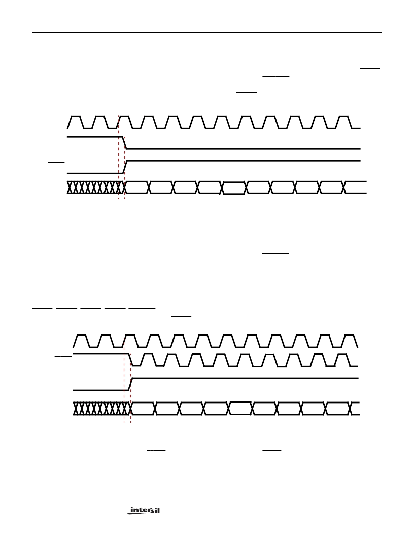
FIGURE 8. OUTPUT TIMING FOR 8-BIT YCbCr MODE (DVLD_LTC = 0)
CLK
DVALID
P[15-8]
t
DVLD
Cb
0
Y
0
Cr
0
Cb
2
Y
2
Cr
2
Y
1
Y
3
Cb
4
Y
4
BLANK
CLK
DVALID
P[15-8]
t
DVLD
Cb
0
Y
0
Cr
0
Cb
2
Y
2
Cr
2
Y
1
Y
3
Cb
4
NOTES:
6. Y
0
is the first active luminance pixel data of a line. Cb
0
and Cr
0
are first active chrominance pixel data in a line. Cb and Cr will alternate every
cycle due to the 4:2:2 subsampling. Pixel data is not output during the blanking period, but the values are forced to blanking levels.
7. When DVLD_LTC is set to 1, the polarity of DVALID needs to be set to active low, otherwise DVALID will stay low during active video and be
gated with the clock only during the blanking interval.
FIGURE 9. OUTPUT TIMING FOR 8-BIT YCbCr MODE (DVLD_LTC = 1)
Y
4
BLANK
HMP8117
相關PDF資料 |
PDF描述 |
|---|---|
| HMP8117CN | NTSC/PAL Video Decoder |
| HMP8154 | NTSC/PAL Encoders |
| HMP8154CN | NTSC/PAL Encoders |
| HMP8156A | NTSC/PAL Encoders |
| HMP8154EVAL1 | NTSC/PAL Encoders |
相關代理商/技術參數 |
參數描述 |
|---|---|
| HMP8117_07 | 制造商:INTERSIL 制造商全稱:Intersil Corporation 功能描述:NTSC/PAL Video Decoder |
| HMP8117CN | 功能描述:編碼器、解碼器、復用器和解復用器 80PQFP,0+70C NTSC/PAL VIDEO DECODER W/MA RoHS:否 制造商:Micrel 產品:Multiplexers 邏輯系列:CMOS 位數: 線路數量(輸入/輸出):2 / 12 傳播延遲時間:350 ps, 400 ps 電源電壓-最大:2.625 V, 3.6 V 電源電壓-最小:2.375 V, 3 V 最大工作溫度:+ 85 C 安裝風格:SMD/SMT 封裝 / 箱體:QFN-44 封裝:Tray |
| HMP8117CN96 | 制造商:Rochester Electronics LLC 功能描述:- Bulk |
| HMP8117CNZ | 功能描述:編碼器、解碼器、復用器和解復用器 W/ANNEAL 80PQFP 0+70 DECODER W/MA RoHS:否 制造商:Micrel 產品:Multiplexers 邏輯系列:CMOS 位數: 線路數量(輸入/輸出):2 / 12 傳播延遲時間:350 ps, 400 ps 電源電壓-最大:2.625 V, 3.6 V 電源電壓-最小:2.375 V, 3 V 最大工作溫度:+ 85 C 安裝風格:SMD/SMT 封裝 / 箱體:QFN-44 封裝:Tray |
| HMP8154 | 制造商:INTERSIL 制造商全稱:Intersil Corporation 功能描述:NTSC/PAL Encoders |
發布緊急采購,3分鐘左右您將得到回復。