- 您現(xiàn)在的位置:買賣IC網(wǎng) > PDF目錄385391 > HS-26C(T)32RH (Intersil Corporation) () PDF資料下載
參數(shù)資料
| 型號: | HS-26C(T)32RH |
| 廠商: | Intersil Corporation |
| 英文描述: | () |
| 中文描述: | () |
| 文件頁數(shù): | 3/4頁 |
| 文件大小: | 35K |
| 代理商: | HS-26C(T)32RH |
4-3
System Noise
Another primary benefit of a balanced, differential line stan-
dard such as RS-422 is the cancellation of radiated EMI
from the data lines. A shielded twisted-pair data line has pri-
mary EMI cancellation by virtue of the anti-phase signals
and Faraday shielding as well. In applications where sensi-
tive analog circuitry has to reside near the data bus, this type
of bus standard can significantly improve system noise lev-
els and signal quality.
Using this chip set, a 10MHz, low power, quiet bus system
with cross-strapped redundant data paths can be imple-
mented easily. The Intersil radiation-hardened CMOS solu-
tion cuts power compared to bipolar chip sets and allows
configurations not possible with standard CMOS logic.
The large voltage swings, low typical line impedance and dif-
ferential bus also provide superior immunity to both supply
and radiatively-coupled noise. The normal signal span is 8V
(+4 to -4) for the HS-26C31/32RH, less than 5V for standard
single-ended CMOS and less than 4V for LSTTL. In addition,
the HS-26C32RH can tolerate differences between driver
and receiver ground levels which would render standard
logic either unreliable or completely nonfunctional. For
example, an LSTTL or CMOS input whose ground supply is
more than 1V below the driving device’s may never switch
because its VIL(min) level cannot be met. The HS-26C32RH
functions properly with its inputs
±
7V from device ground.
This also minimizes the chances of ground bounce or supply
spikes causing false logic states.
Substrate Connection
The substrate of the HS-26C(T)32RH circuits is connected
internally to the VDD pin. If the ’32 is used in die form for
hybrid applications, the die should be mounted to an electri-
cally isolated surface. If there is any electrical connection to
the back side of the die there will be a low value resistance
to the VDD pin. However, the value of the resistance of the
substrate and mounting material are not necessarily low or
well enough controlled to use as a supply feed.
Power Dissipation
The HS-26C(T)32RH dissipates about 15mA IDD current at
standby. About half of this is used by the divider network and
the balance by the input comparators’ analog circuitry.
Operating current at frequency is the sum of the standby cur-
rent and the dynamic operating current given by (CPD)
(VDD) (frequency). For the HS-26C(T)32RH the CPD (per
active channel) is 40pF. This is equivalent to other ’32 types.
Input Fail Safe
The HS-26C(T)32RH is designed to produce a logic “1” out-
put state when the transmission line inputs are open. This is
a special case fault tolerance feature. The failsafe works by
a designed imbalance in the input resistor structure, which
produces an inherent error voltage when the inputs are high
impedance. The error voltage must be greater than the mini-
mum input differential signal.
Failsafe operation depends on a true high impedance condi-
tion at the inputs. Some circuit or termination schemes may
mask or reduce effectiveness of the failsafe mechanism if
they produce a low impedance across the input terminals.
The minimum impedance permissible for adequate failsafe
operation is that which results in an input differential voltage
of 400mV, the worst case VTH(in).
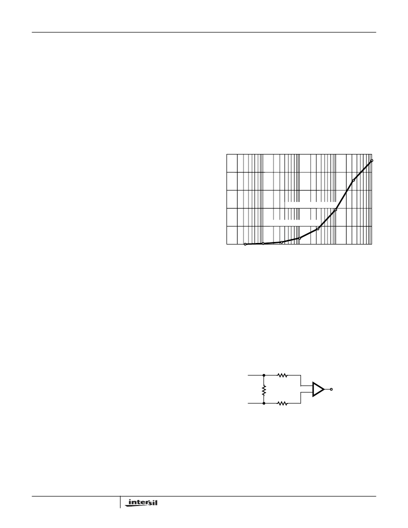
The relationship between input failsafe differential voltage
and external input impedance is shown below. In order to
produce an acceptable differential under an open-line fault
condition, any input network external to the chip must
present no less than 10k
to the line inputs. See plot in
Figure 4.
FIGURE 4. INPUT FAIL SAFE DIFFERENTIAL vs ZIN (OPEN)
The practice of simple resistor shunt termination (100
across lines) will inhibit failsafe operation because the shunt
resistor will mask the open line condition. If a shunt termina-
tion scheme is to be used, it becomes necessary to design a
termination which restores the differential bias to the front
end. The schematic on the next page shows one possible
implementation.
Figure 5 produces too small an input differential voltage in
the open-line fault condition. The internal input bias network
is shunted by the termination resistor.
FIGURE 5.
Figure 6 produces an adequate input differential voltage in
the open-line fault condition. The internal input bias network
is supplemented externally to compensate for the termina-
tion resistor.
1.0
0.80
0.60
0.40
0.20
0.0
10
1
10
2
10
3
10
4
10
5
VTH(IN)
≤
400mV MAX
VTH(IN)
≤
200mV TYP
INP
INM
26C32MIN
OUT
100
R21
R23
100
100
R22
+
-
Application Note 9520
相關(guān)PDF資料 |
PDF描述 |
|---|---|
| HS-26C31RH-T | Radiation Hardened Quad Differential Line Receiver(抗輻射四路差分線接收器) |
| HS-26CLV31RH | Radiation Hardened 3.3V Quad Differential Line Driver |
| HS1-26CLV31RH-8 | Radiation Hardened 3.3V Quad Differential Line Driver |
| HS9-26CLV31RH-8 | Radiation Hardened 3.3V Quad Differential Line Driver |
| HS0-26CLV31RH-Q | Radiation Hardened 3.3V Quad Differential Line Driver |
相關(guān)代理商/技術(shù)參數(shù) |
參數(shù)描述 |
|---|---|
| HS-26CT32RH-T | 制造商:INTERSIL 制造商全稱:Intersil Corporation 功能描述:Radiation Hardened Quad Differential Line Receiver |
| HS27 | 功能描述:散熱片 Heatsink, PSIP RoHS:否 制造商:Ampro By ADLINK 產(chǎn)品:Heat Sink Accessories 安裝風(fēng)格:Through Hole 散熱片材料: 散熱片樣式: 熱阻: 長度: 寬度: 高度: 設(shè)計目的:Express-HRR |
| HS-2700RH | 制造商:INTERSIL 制造商全稱:Intersil Corporation 功能描述:Low Power, High Performance Radiation Hardened Operational Amplifier |
| HS271 | 功能描述:散熱片 2.7 C/W PM Heat Sink 1 SSR RoHS:否 制造商:Ampro By ADLINK 產(chǎn)品:Heat Sink Accessories 安裝風(fēng)格:Through Hole 散熱片材料: 散熱片樣式: 熱阻: 長度: 寬度: 高度: 設(shè)計目的:Express-HRR |
| HS271DR | 功能描述:散熱片 2.7 C/W DIN RM Heat Sink - 1 SSR RoHS:否 制造商:Ampro By ADLINK 產(chǎn)品:Heat Sink Accessories 安裝風(fēng)格:Through Hole 散熱片材料: 散熱片樣式: 熱阻: 長度: 寬度: 高度: 設(shè)計目的:Express-HRR |
發(fā)布緊急采購,3分鐘左右您將得到回復(fù)。