- 您現在的位置:買賣IC網 > PDF目錄385393 > HS1-81C55RH-Q (INTERSIL CORP) Radiation Hardened 256 x 8 CMOS RAM PDF資料下載
參數資料
| 型號: | HS1-81C55RH-Q |
| 廠商: | INTERSIL CORP |
| 元件分類: | DRAM |
| 英文描述: | Radiation Hardened 256 x 8 CMOS RAM |
| 中文描述: | 256 X 8 MULTI-PORT SRAM, CDIP40 |
| 封裝: | SIDE BRAZED, CERAMIC, DIP-40 |
| 文件頁數: | 3/11頁 |
| 文件大小: | 122K |
| 代理商: | HS1-81C55RH-Q |
3
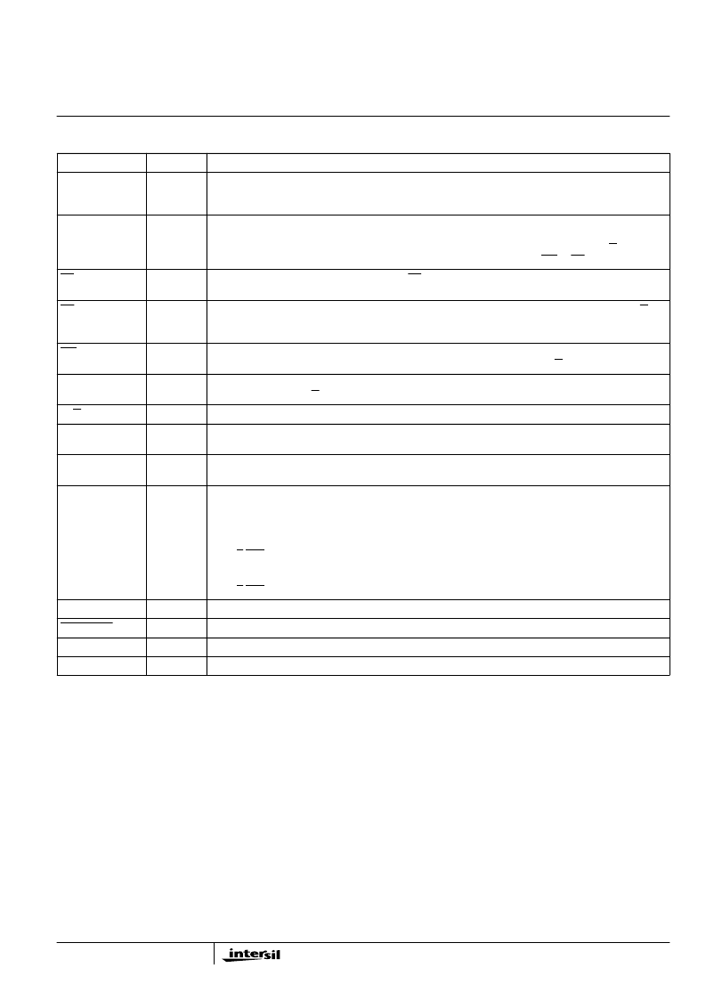
Pin Descriptions
SYMBOL
TYPE
NAME AND FUNCTION
RESET
I
Reset:
Pulse provided by the HS-80C85RH to initialize the system (connect to HS-80C85RH RESET OUT).
Input high on this line resets the chip and initializes the three I/O ports to input mode. The width of RESET
pulse should typically be two HS-80C85RH clock cycle times.
AD0 - AD7
I/O
Address/Data:
Three-state Address/Data lines that interface with the CPU lower 8-bit Address/Data Bus. The
8-bit address is latched into the address latch inside the HS-81C55 and HS-81C56RH on the falling edge of
ALE. The address can be either for the memory section or the I/O section depending on the IO/M input. The
8-bit data is either written into the chip or read from the chip, depending on the WR or RD input signal.
CE or CE
I
Chip Enable:
On the HS-81C55RH, this pin is CE and is ACTIVE LOW. On the HS-81C56RH, this pin is CE
and is ACTIVE HIGH.
RD
I
Read Control:
Input low on this line with the Chip Enable active enables and AD0 - AD7 buffers. If IO/M pin
is low, the RAM content will be read out to the AD bus. Otherwise the content of the selected I/O port or
command/status registers will be read to the AD bus.
WR
I
Write Control:
Input low on this line with the Chip Enable active causes the data on the Address/Data bus to
be written to the RAM or I/O ports and command/status register, depending on IO/M.
ALE
I
Address Latch Enable:
This control signal latches both the address on the AD0 - AD7 lines and the state of
the Chip Enable and IO/M into the chip at the falling edge of ALE.
IO/M
I
I/O Memory:
Selects memory if low and I/O and command/status registers if high.
PA0 - PA7 (8)
I/O
Port A:
These 8 pins are general purpose I/O pins. The in/out direction is selected by programming the
command register.
PB0 - PB7 (8)
I/O
Port B:
These 8 pins are general purpose I/O pins. The in/out direction is selected by programming the
command register.
PC0 - PC7 (8)
I/O
Port C:
These 6 pins can function as either input port, output port, or as control signals for PA and PB.
Programming is done through the command register. When PC0 - PC5 are used as control signals, they will
provide the following:
PC0 - A INTR (Port A Interrupt)
PC1 - ABF (Port A Buffer Full)
PC2 - A STB (Port A Strobe)
PC3 - B INTR (Port B Interrupt)
PC4 - B BF (Port B Buffer Full)
PC5 - B STB (Port B Strobe)
TIMER IN
I
Timer Input:
Input to the counter-timer.
TIMER OUT
O
Timer Output:
This output can be either a square wave or a pulse, depending on the timer mode.
VDD
I
Voltage:
+5V.
GND
I
Ground:
Ground reference.
HS-81C55RH, HS-81C56RH
相關PDF資料 |
PDF描述 |
|---|---|
| HS1-81C56RH-8 | Radiation Hardened 256 x 8 CMOS RAM |
| HS1-81C56RH-Q | Radiation Hardened 256 x 8 CMOS RAM |
| HS1100 | RELATIVE HUMIDITY SENSOR |
| HS1101 | RELATIVE HUMIDITY SENSOR |
| HS13 | HIGH EFFICIENCY RECTIFIERS(1.0A,50-400V) |
相關代理商/技術參數 |
參數描述 |
|---|---|
| HS1-81C56RH | 制造商:INTERSIL 制造商全稱:Intersil Corporation 功能描述:Radiation Hardened 256 x 8 CMOS RAM |
| HS1-81C56RH-8 | 制造商:INTERSIL 制造商全稱:Intersil Corporation 功能描述:Radiation Hardened 256 x 8 CMOS RAM |
| HS1-81C56RH-Q | 制造商:INTERSIL 制造商全稱:Intersil Corporation 功能描述:Radiation Hardened 256 x 8 CMOS RAM |
| HS1820A | 制造商:未知廠家 制造商全稱:未知廠家 功能描述:Peripheral IC |
| HS1820B | 制造商:未知廠家 制造商全稱:未知廠家 功能描述:Peripheral IC |
發布緊急采購,3分鐘左右您將得到回復。