- 您現在的位置:買賣IC網 > PDF目錄385398 > HT27C040 (Holtek Semiconductor Inc.) 512K x 8-Bit CMOS OTP EPROM(512K x 8位 CMOS一次可編程EPROM) PDF資料下載
參數資料
| 型號: | HT27C040 |
| 廠商: | Holtek Semiconductor Inc. |
| 英文描述: | 512K x 8-Bit CMOS OTP EPROM(512K x 8位 CMOS一次可編程EPROM) |
| 中文描述: | 為512k × 8位檢察官辦公室的CMOS存儲器(為512k × 8位的CMOS一次可編程存儲器) |
| 文件頁數: | 3/10頁 |
| 文件大小: | 110K |
| 代理商: | HT27C040 |
Absolute Maximum Rating
Operation Temperature Commercial..................................................................................0 C to +70 C
Storage Temperature....................................................................................................... 65 C to 125 C
Applied VCC Voltage with Respect to VSS ...................................................................... 0.6V to 7.0V
Applied Voltage on Input Pin with Respect to VSS......................................................... 0.6V to 7.0V
Applied Voltage on Output Pin with Respect to VSS.............................................. 0.6V to V
CC
+0.5V
Applied Voltage on A9 Pin with Respect to VSS............................................................ 0.6V to 13.5V
Applied VPP Voltage with Respect to VSS...................................................................... 0.6V to 13.5V
Applied READ Voltage (Functionality is guaranteed between these limits)................+4.5V to +5.5V
Note: These are stress ratings only. Stresses exceeding the range specified under Absolute Maxi-
mumRatings maycausesubstantialdamagetothedevice.Functionaloperationofthisdevice
at other conditions beyond those listed in the specification is not implied and prolonged expo-
sure to extreme conditions may affect device reliability.
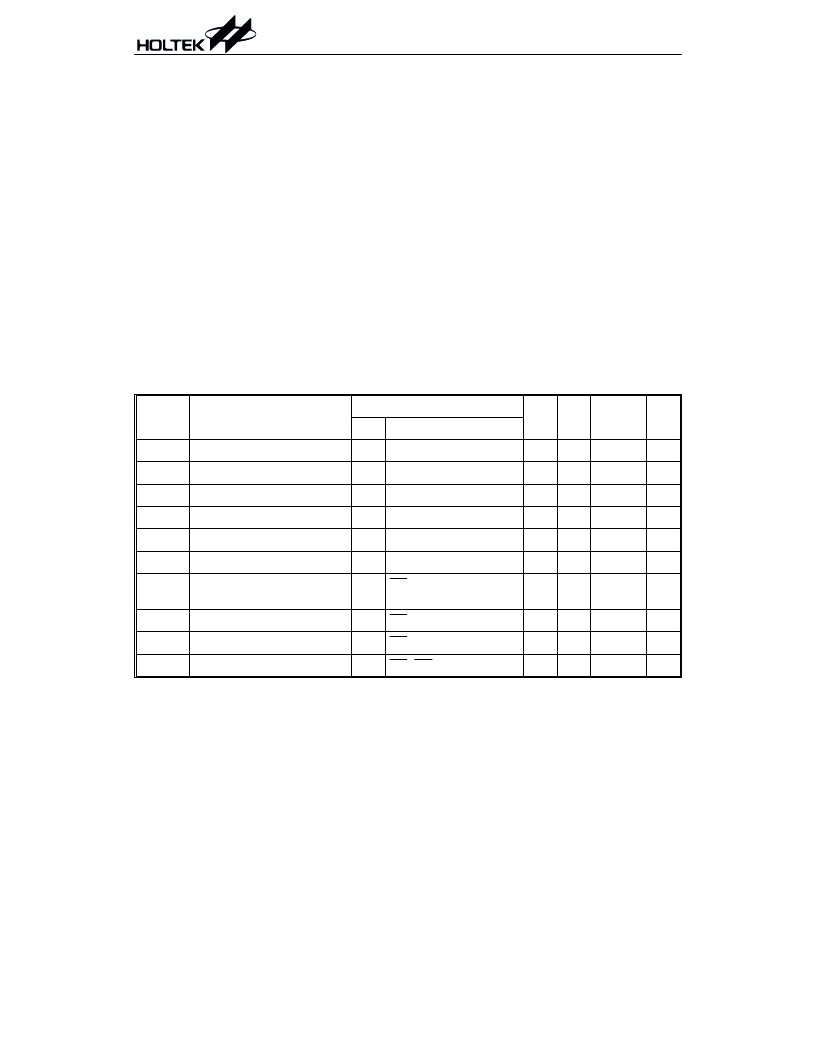
D.C. Characteristics
Read operation
Symbol
Parameter
Test Conditions
Min. Typ.
Max.
Unit
V
CC
Conditions
V
OH
Output High Level
5V
I
OH
= 0.4mA
2.4
V
V
OL
Output Low Level
5V
I
OL
=2.1mA
0.45
V
V
IH
Input High Level
5V
2.0
V
CC
+0.5
V
V
IL
Input Low Level
5V
0.3
0.8
V
I
LI
Input Leakage Current
5V
V
IN
=0 to 5.5V
5
5
A
I
LO
Output Leakage Current
5V
V
OUT
=0 to 5.5V
10
10
A
I
CC
VCC Active Current
5V
CE=V
IL
, f=5MHz,
I
OUT
=0mA
30
mA
I
SB1
Standby Current (CMOS)
5V
CE=V
CC
0.3V
1.0
10
A
I
SB2
Standby Current (TTL)
5V
CE=V
IH
1.0
mA
I
PP
VPP Read/Standby Current
5V
CE=OE=V
IL
, V
PP
=V
CC
100
A
Preliminary
HT27C040
3
August 29, 2000
相關PDF資料 |
PDF描述 |
|---|---|
| HT27C512 | OTP CMOS 64Kx 8-Bit EPROM |
| HT27LC010 | CMOS 128K X 8-Bit OTP EPROM |
| HT27LC020 | OTP CMOS 256Kx 8-Bit EPROM |
| HT27LC040 | CMOS 512K 8-Bit OTP EPROM |
| HT27LC512 | OTP CMOS 64Kx 8-Bit EPROM |
相關代理商/技術參數 |
參數描述 |
|---|---|
| HT27C4096 | 制造商:未知廠家 制造商全稱:未知廠家 功能描述:CMOS 256K?16-Bit OTP EPROM ??(5V) |
| HT27C512 | 制造商:HOLTEK 制造商全稱:Holtek Semiconductor Inc 功能描述:OTP CMOS 64Kx 8-Bit EPROM |
| HT27C512(28DIP)-45 | 制造商:未知廠家 制造商全稱:未知廠家 功能描述:x8 EPROM |
| HT27C512(28DIP)-70 | 制造商:未知廠家 制造商全稱:未知廠家 功能描述:x8 EPROM |
| HT27C512(28DIP)-90 | 制造商:未知廠家 制造商全稱:未知廠家 功能描述:x8 EPROM |
發布緊急采購,3分鐘左右您將得到回復。