- 您現在的位置:買賣IC網 > PDF目錄385414 > HY27UAxxx (Hynix Semiconductor Inc.) 1Gbit (128Mx8bit / 64Mx16bit) NAND Flash Memory PDF資料下載
參數資料
| 型號: | HY27UAxxx |
| 廠商: | Hynix Semiconductor Inc. |
| 英文描述: | 1Gbit (128Mx8bit / 64Mx16bit) NAND Flash Memory |
| 中文描述: | 1Gbit的(128Mx8bit / 64Mx16bit)NAND閃存 |
| 文件頁數: | 25/43頁 |
| 文件大小: | 729K |
| 代理商: | HY27UAXXX |
第1頁第2頁第3頁第4頁第5頁第6頁第7頁第8頁第9頁第10頁第11頁第12頁第13頁第14頁第15頁第16頁第17頁第18頁第19頁第20頁第21頁第22頁第23頁第24頁當前第25頁第26頁第27頁第28頁第29頁第30頁第31頁第32頁第33頁第34頁第35頁第36頁第37頁第38頁第39頁第40頁第41頁第42頁第43頁
Rev 0.5 / Oct. 2004
25
HY27UA(08/16)1G1M Series
HY27SA(08/16)1G1M Series
1Gbit (128Mx8bit / 64Mx16bit) NAND Flash
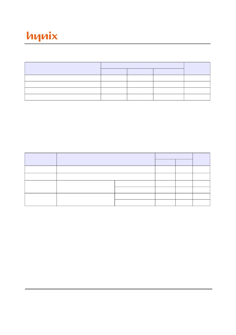
Table 9: Program, Erase Time and Program Erase Endurance Cycles
MAXIMUM RATING
Stressing the device above the ratings listed in Table 10, Absolute Maximum Ratings, may cause permanent damage to
the device. These are stress ratings only and operation of the device at these or any other conditions above those indi-
cated in the Operating sections of this specification is not implied. Exposure to Absolute Maximum Rating conditions
for extended periods may affect device reliability.
Table 10: Absolution Maximum Rating
Note: (1). Minimum Voltage may undershoot to -2V for less than 20ns during transitions on input and I/O pins. Maximum voltage
may overshoot to V
CC
+ 2V for less than 20ns during transitions on I/O pins.
DC AND AC PARAMETERS
This section summarizes the operating and measurement conditions, and the DC and AC characteristics of the device.
The parameters in the DC and AC characteristics Tables that follow, are derived from tests performed under the Mea-
surement Conditions summarized in Table 11, Operating and AC Measurement Conditions. Designers should check that
the operating conditions in their circuit match the measurement conditions when relying on the quoted parameters.
Parameters
NAND Flash
Unit
Min
Typ
Max
Page Program Time
200
500
us
Block Erase Time
2
3
ms
Program/Erase Cycles (per block)
100,000
cycles
Data Retention
10
years
Symbol
Parameter
NAND Flash
Unit
Min
Max
T
BIAS
Temperature Under Bias
-50
125
o
C
T
STG
Storage Temperature
-65
150
o
C
V
IO(1)
Input or Output Voltage
1.8V devices
-0.6
2.7
V
3.3 V devices
-0.6
4.6
V
V
CC
Supply Voltage
1.8V devices
-0.6
2.7
V
3.3 V devices
-0.6
4.6
V
相關PDF資料 |
PDF描述 |
|---|---|
| HY27SS08561M | 256Mbit (32Mx8bit / 16Mx16bit) NAND Flash |
| HY27SS561M | 256Mbit (32Mx8bit / 16Mx16bit) NAND Flash |
| HY27US16561M | 256Mbit (32Mx8bit / 16Mx16bit) NAND Flash |
| HY27US561M | 256Mbit (32Mx8bit / 16Mx16bit) NAND Flash |
| HY27SS16561M | 256Mbit (32Mx8bit / 16Mx16bit) NAND Flash |
相關代理商/技術參數 |
參數描述 |
|---|---|
| HY27UF081G2A | 制造商:HYNIX 制造商全稱:Hynix Semiconductor 功能描述:1Gbit (128Mx8bit / 64Mx16bit) NAND Flash |
| HY27UF081G2A-C | 制造商:SK Hynix Inc 功能描述: |
| HY27UF081G2A-F(P) | 制造商:SK Hynix Inc 功能描述: |
| HY27UF081G2A-S(P) | 制造商:SK Hynix Inc 功能描述: |
| HY27UF081G2A-T(P) | 制造商:SK Hynix Inc 功能描述: |
發布緊急采購,3分鐘左右您將得到回復。