- 您現在的位置:買賣IC網 > PDF目錄360751 > ICS570MIT Multiplier and Zero Delay Buffer PDF資料下載
參數資料
| 型號: | ICS570MIT |
| 英文描述: | Multiplier and Zero Delay Buffer |
| 中文描述: | 乘數和零延遲緩沖器 |
| 文件頁數: | 1/6頁 |
| 文件大小: | 85K |
| 代理商: | ICS570MIT |
ICS570A
Multiplier and Zero Delay Buffer
MDS 570A C
Integrated Circuit Systems, Inc . 525 Race Street San Jose CA 95126 (408)295-9800tel www.icst.com
1
Revision 102700
Printed 11/14/00
Packaged in 8 pin SOIC.
Pin-for-pin replacement and upgrade to ICS570
Functional equivalent to AV9170 (not a pin-
for-pin replacement).
Low input to output skew of 500 ps max.
Low skew (250 ps) outputs. One is ÷ 2 of other.
Ability to choose between 14 different
multipliers from 0.5X to 32X.
Input clock frequency up to 150 MHz at 3.3V.
Can recover poor input clock duty cycle.
Output clock duty cycle of 45/55.
Power Down and Tri-State Mode.
Full CMOS clock swings with 25mA drive
capability at TTL levels.
Advanced, low power CMOS process.
Operating voltage of 3.0 to 5.5 V.
Industrial temperature version available
The ICS570A is a high performance Zero Delay
Buffer (ZDB) which integrates ICS’ proprietary
analog/digital Phase Locked Loop (PLL) techniques.
ICS introduced the world standard for these devices
in 1992 with the debut of the AV9170. The
ICS570A, part of ICS’ ClockBlocks
family, was
designed as a performance upgrade to meet today’s
higher speed and lower voltage requirements. The
zero delay feature means that the rising edge of the
input clock aligns with the rising edges of both
outputs, giving the appearance of no delay through
the device. There are two outputs on the chip, one
being a low-skew divide by two of the other. The chip
has an all-chip power down/tri-state mode that stops
the internal PLL and puts both outputs into the high
impedance state.
The chip is ideal for synchronizing outputs in a large
variety of systems, from personal computers to data
communications to video. By allowing off-chip
feedback paths, the ICS570A can eliminate the delay
through other devices.
The ICS570A was done to improve jitter from the
original ICS570, and so it is recommended for all new
designs.
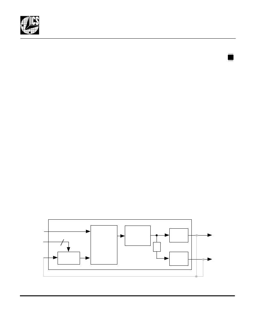
Block Diagram
Description
Features
divide by
N
Phase
Detector,
Charge
Pump, and
Loop Filter
Voltage
Controlled
Oscillator
CLK
Output
Buffer
ICLK
S1, S0
CLK/2
Output
Buffer
FBIN
÷2
2
External feedback can come from CLK or CLK/2 (see table on page 2).
相關PDF資料 |
PDF描述 |
|---|---|
| ICS570MT | Multiplier and Zero Delay Buffer |
| ICS570B | Multiplier and Zero Delay Buffer |
| ICS570BI | Multiplier and Zero Delay Buffer |
| ICS570BIT | Multiplier and Zero Delay Buffer |
| ICS570BT | Multiplier and Zero Delay Buffer |
相關代理商/技術參數 |
參數描述 |
|---|---|
| ICS570MT | 制造商:ICS 制造商全稱:ICS 功能描述:Multiplier and Zero Delay Buffer |
| ICS571 | 制造商:ICS 制造商全稱:ICS 功能描述:Low Phase Noise Zero Delay Buffer |
| ICS571M | 功能描述:IC MULTIPLIER/ZDB 8-SOIC RoHS:否 類別:集成電路 (IC) >> 時鐘/計時 - 時鐘發生器,PLL,頻率合成器 系列:ClockBlocks™ 產品變化通告:Product Discontinuation 04/May/2011 標準包裝:96 系列:- 類型:時鐘倍頻器,零延遲緩沖器 PLL:帶旁路 輸入:LVTTL 輸出:LVTTL 電路數:1 比率 - 輸入:輸出:1:8 差分 - 輸入:輸出:無/無 頻率 - 最大:133.3MHz 除法器/乘法器:是/無 電源電壓:3 V ~ 3.6 V 工作溫度:0°C ~ 70°C 安裝類型:表面貼裝 封裝/外殼:16-TSSOP(0.173",4.40mm 寬) 供應商設備封裝:16-TSSOP 包裝:管件 其它名稱:23S08-5HPGG |
| ICS571MLF | 功能描述:IC ZDB LOW PHASE NOISE 8-SOIC RoHS:是 類別:集成電路 (IC) >> 時鐘/計時 - 時鐘發生器,PLL,頻率合成器 系列:ClockBlocks™ 標準包裝:2,000 系列:- 類型:PLL 頻率合成器 PLL:是 輸入:晶體 輸出:時鐘 電路數:1 比率 - 輸入:輸出:1:1 差分 - 輸入:輸出:無/無 頻率 - 最大:1GHz 除法器/乘法器:是/無 電源電壓:4.5 V ~ 5.5 V 工作溫度:-20°C ~ 85°C 安裝類型:表面貼裝 封裝/外殼:16-LSSOP(0.175",4.40mm 寬) 供應商設備封裝:16-SSOP 包裝:帶卷 (TR) 其它名稱:NJW1504V-TE1-NDNJW1504V-TE1TR |
| ICS571MLFT | 功能描述:IC BUFFER ZD LOW PH/NOISE 8-SOIC RoHS:是 類別:集成電路 (IC) >> 時鐘/計時 - 時鐘發生器,PLL,頻率合成器 系列:ClockBlocks™ 標準包裝:2,000 系列:- 類型:PLL 時鐘發生器 PLL:帶旁路 輸入:LVCMOS,LVPECL 輸出:LVCMOS 電路數:1 比率 - 輸入:輸出:2:11 差分 - 輸入:輸出:是/無 頻率 - 最大:240MHz 除法器/乘法器:是/無 電源電壓:3.135 V ~ 3.465 V 工作溫度:0°C ~ 70°C 安裝類型:表面貼裝 封裝/外殼:32-LQFP 供應商設備封裝:32-TQFP(7x7) 包裝:帶卷 (TR) |
發布緊急采購,3分鐘左右您將得到回復。