- 您現在的位置:買賣IC網 > PDF目錄79611 > ICS9214DGLF-T (INTEGRATED DEVICE TECHNOLOGY INC) 9214 SERIES, PLL BASED CLOCK DRIVER, 4 TRUE OUTPUT(S), 0 INVERTED OUTPUT(S), PDSO28 PDF資料下載
參數資料
| 型號: | ICS9214DGLF-T |
| 廠商: | INTEGRATED DEVICE TECHNOLOGY INC |
| 元件分類: | 時鐘及定時 |
| 英文描述: | 9214 SERIES, PLL BASED CLOCK DRIVER, 4 TRUE OUTPUT(S), 0 INVERTED OUTPUT(S), PDSO28 |
| 封裝: | 0.173 INCH, 0.65 MM PITCH, LEAD FREE, MO-153, TSSOP-28 |
| 文件頁數: | 1/18頁 |
| 文件大小: | 310K |
| 代理商: | ICS9214DGLF-T |
Integrated
Circuit
Systems, Inc.
ICS9214
0809E–11/17/06
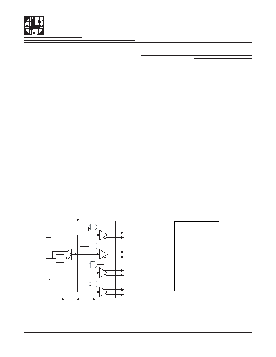
Block Diagram
Rambus
TM
XDR
TM
Clock Generator
The ICS9214 clock generator provides the necessary clock
signals to support the Rambus XDR
TM memory subsystem
and Redwood logic interface. The clock source is a reference
clock that may or may not be modulated for spread spectrum.
The ICS9214 provides 4 differential clock pairs in a space
saving 28-pin TSSOP package and provides an off-the-shelf
high-performance interface solution.
Figure 1 shows the major components of the ICS9214 XDR
Clock Generator.
These include the a PLL, a Bypass
Multiplexer and four differential output buffers. The outputs
can be disabled by a logic low on the OE pin. An output is
enabled by the combination of the OE pin being high, and 1
in its SMBus Output control register bit.
The PLL receives a reference clock, CLK_INT/C and outputs
a clock signal at a frequency equal to the input frequency
times a multiplier. Table 2 shows the multipliers selectable
via the SMBus interface. This clock signal is then fed to the
differential output buffers to drive the enabled clocks. Disabled
outputs are set to Hi-Z. The Bypass mode routes the input
clock, CLK_INT/C, directly to the differential output buffers,
bypassing the PLL.
Up to four ICS9214 devices can be cascaded on the same
SMBus. Table 3 shows the SMBus addressing and control for
the four devices.
400 – 500 MHz clock source
4 open-drain differential output drives with short term
jitter < 40ps
Spread spectrum compatible
Reference clock is differential or single-ended, 100 or
133 MHz
SMBus programmability for:
- frequency multiplier
- output enable
- operating mode
Supports frequency multipliers of: 3, 4, 5, 6, 8,
9/2,
15/2 and 15/4
Support systems where XDR subsystem is
asynchronous to other system clocks
2.5V power supply
PLL
Bypass
MUX
RegA
RegB
RegC
RegD
CLK_INT
CLK_INC
SMBCLK
OE
BYPASS#/PLL
SMBDAT SMB_A0 SMB_A1
ODCLK_C3
ODCLK_T3
ODCLK_C2
ODCLK_T2
ODCLK_C1
ODCLK_T1
ODCLK_C0
ODCLK_T0
AVDD2.5
1
28 VDD2.5
AGND
2
27 ODCLK_T0
IREFY
3
26 ODCLK_C0
AGND
4
25 GND
CLK_INT
5
24 ODCLK_T1
CLK_INC
6
23 ODCLK_C1
VDD2.5
7
22 VDD2.5
GND
8
21 GND
SMBCLK
9
20 ODCLK_T2
SMBDAT 10
19 ODCLK_C2
OE 11
18 GND
SMB_A0 12
17 ODCLK_T3
SMB_A1 13
16 ODCLK_C3
BYPASS#/PLL 14
15 VDD2.5
IC
S
921
4
Pin Configuration
28-Pin 4.4mm TSSOP
General Description
Features
相關PDF資料 |
PDF描述 |
|---|---|
| ICS9214DGLF | 9214 SERIES, PLL BASED CLOCK DRIVER, 4 TRUE OUTPUT(S), 0 INVERTED OUTPUT(S), PDSO28 |
| ICS95V857AH-T | 95V SERIES, PLL BASED CLOCK DRIVER, 10 TRUE OUTPUT(S), 0 INVERTED OUTPUT(S), PBGA56 |
| ICS9112AM-16LFT | 9112 SERIES, PLL BASED CLOCK DRIVER, 5 TRUE OUTPUT(S), 0 INVERTED OUTPUT(S), PDSO8 |
| ICS9112AM-27LFT | 9112 SERIES, LOW SKEW CLOCK DRIVER, 4 TRUE OUTPUT(S), 0 INVERTED OUTPUT(S), PDSO8 |
| I74F657D,112 | F/FAST SERIES, 8-BIT TRANSCEIVER, TRUE OUTPUT, PDSO24 |
相關代理商/技術參數 |
參數描述 |
|---|---|
| ICS9214YGLF-T | 制造商:ICS 制造商全稱:ICS 功能描述:Rambus XDR Clock Generator |
| ICS9219 | 制造商:ICS 制造商全稱:ICS 功能描述:Direct Rambus Clock Generator Lite |
| ICS9219YGLF-T | 制造商:ICS 制造商全稱:ICS 功能描述:Direct Rambus Clock Generator Lite |
| ICS9220 | 制造商:IDT 制造商全稱:Integrated Device Technology 功能描述:Programmable RambusTM XDRTM Clock Generator |
| ICS9220B | 制造商:IDT 制造商全稱:Integrated Device Technology 功能描述:Programmable RambusTM XDRTM Clock Generator |
發布緊急采購,3分鐘左右您將得到回復。