- 您現(xiàn)在的位置:買賣IC網(wǎng) > PDF目錄360929 > IRF540FI (意法半導體) N - CHANNEL100V - 00.50ohm - 30A - TO-220/TO-220FI POWER MOSFET PDF資料下載
參數(shù)資料
| 型號: | IRF540FI |
| 廠商: | 意法半導體 |
| 英文描述: | N - CHANNEL100V - 00.50ohm - 30A - TO-220/TO-220FI POWER MOSFET |
| 中文描述: | ? - CHANNEL100V - 00.50ohm - 30A條- TO-220/TO-220FI的功率MOSFET |
| 文件頁數(shù): | 2/9頁 |
| 文件大小: | 86K |
| 代理商: | IRF540FI |
Philips Semiconductors
Product specification
N-channel TrenchMOS
transistor
IRF540, IRF540S
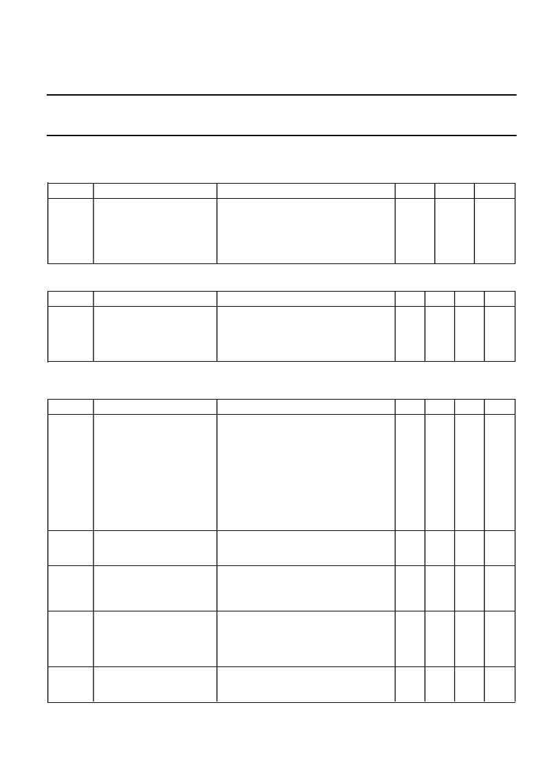
AVALANCHE ENERGY LIMITING VALUES
Limiting values in accordance with the Absolute Maximum System (IEC 134)
SYMBOL PARAMETER
E
AS
Non-repetitive avalanche
energy
CONDITIONS
Unclamped inductive load, I
= 10 A;
t
p
= 350
μ
s; T
j
prior to avalanche = 25C;
V
≤
25 V; R
GS
= 50
; V
GS
= 10 V; refer
to fig:14
MIN.
-
MAX.
230
UNIT
mJ
I
AS
Peak non-repetitive
avalanche current
-
23
A
THERMAL RESISTANCES
SYMBOL PARAMETER
R
th j-mb
Thermal resistance junction
to mounting base
R
th j-a
Thermal resistance junction
to ambient
CONDITIONS
MIN.
-
TYP. MAX. UNIT
-
1.5
K/W
SOT78 package, in free air
SOT404 package, pcb mounted, minimum
footprint
-
-
60
50
-
-
K/W
K/W
ELECTRICAL CHARACTERISTICS
T
j
= 25C unless otherwise specified
SYMBOL PARAMETER
V
(BR)DSS
Drain-source breakdown
voltage
V
GS(TO)
Gate threshold voltage
CONDITIONS
V
GS
= 0 V; I
D
= 0.25 mA;
MIN.
100
89
2
1
-
-
-
8.7
-
-
-
-
-
-
-
-
-
-
-
-
TYP. MAX. UNIT
-
-
-
-
3
4
-
-
-
6
49
77
132
193
15.5
-
10
100
0.05
10
-
250
-
65
-
10
-
29
8
-
39
-
26
-
24
-
3.5
-
4.5
-
V
V
V
V
V
T
j
= -55C
V
DS
= V
GS
; I
D
= 1 mA
T
j
= 175C
T
j
= -55C
R
DS(ON)
Drain-source on-state
resistance
Forward transconductance
Gate source leakage current V
GS
=
±
20 V; V
DS
= 0 V
Zero gate voltage drain
current
Total gate charge
Gate-source charge
Gate-drain (Miller) charge
Turn-on delay time
Turn-on rise time
Turn-off delay time
Turn-off fall time
Internal drain inductance
Internal drain inductance
V
GS
= 10 V; I
D
= 17 A
m
m
S
nA
μ
A
μ
A
nC
nC
nC
ns
ns
ns
ns
nH
nH
T
j
= 175C
g
fs
I
GSS
I
DSS
V
DS
= 25 V; I
= 17 A
V
DS
= 100 V; V
GS
= 0 V
V
DS
= 80 V; V
GS
= 0 V; T
j
= 175C
I
D
= 17 A; V
DD
= 80 V; V
GS
= 10 V
Q
g(tot)
Q
gs
Q
gd
t
d on
t
r
t
d off
t
f
L
d
L
d
V
DD
= 50 V; R
D
= 2.2
;
V
= 10 V; R
G
= 5.6
Resistive load
Measured tab to centre of die
Measured from drain lead to centre of die
(SOT78 package only)
Measured from source lead to source
bond pad
L
s
Internal source inductance
-
7.5
-
nH
C
iss
C
oss
C
rss
Input capacitance
Output capacitance
Feedback capacitance
V
GS
= 0 V; V
DS
= 25 V; f = 1 MHz
-
-
-
890
139
83
1187
167
109
pF
pF
pF
August 1999
2
Rev 1.100
相關PDF資料 |
PDF描述 |
|---|---|
| IRF540 | N - CHANNEL100V - 00.50ohm - 30A - TO-220/TO-220FI POWER MOSFET |
| IRF540NPBF | HEXFET Power MOSFET |
| IRF540 | HEXFET POWER MOSFET |
| IRF540NL | Power MOSFET(Vdss=100V, Rds(on)=44mohm, Id=33A) |
| IRF540NS | Power MOSFET(Vdss=100V, Rds(on)=44mohm, Id=33A) |
相關代理商/技術參數(shù) |
參數(shù)描述 |
|---|---|
| IRF540L | 功能描述:MOSFET N-CH 100V 28A TO-262 RoHS:否 類別:分離式半導體產(chǎn)品 >> FET - 單 系列:- 標準包裝:1,000 系列:MESH OVERLAY™ FET 型:MOSFET N 通道,金屬氧化物 FET 特點:邏輯電平門 漏極至源極電壓(Vdss):200V 電流 - 連續(xù)漏極(Id) @ 25° C:18A 開態(tài)Rds(最大)@ Id, Vgs @ 25° C:180 毫歐 @ 9A,10V Id 時的 Vgs(th)(最大):4V @ 250µA 閘電荷(Qg) @ Vgs:72nC @ 10V 輸入電容 (Ciss) @ Vds:1560pF @ 25V 功率 - 最大:40W 安裝類型:通孔 封裝/外殼:TO-220-3 整包 供應商設備封裝:TO-220FP 包裝:管件 |
| IRF540N | 制造商:International Rectifier 功能描述:MOSFET N TO-220 |
| IRF540N_R4942 | 功能描述:MOSFET TO-220AB N-Ch Power RoHS:否 制造商:STMicroelectronics 晶體管極性:N-Channel 汲極/源極擊穿電壓:650 V 閘/源擊穿電壓:25 V 漏極連續(xù)電流:130 A 電阻汲極/源極 RDS(導通):0.014 Ohms 配置:Single 最大工作溫度: 安裝風格:Through Hole 封裝 / 箱體:Max247 封裝:Tube |
| IRF540N-010HR | 制造商:International Rectifier 功能描述:HI-REL DISCRETE - Rail/Tube |
| IRF540NHR | 制造商:International Rectifier 功能描述:Trans MOSFET N-CH 100V 33A 3-Pin(3+Tab) TO-220AB 制造商:International Rectifier 功能描述:TRANS MOSFET N-CH 100V 33A 3PIN TO-220AB - Rail/Tube |
發(fā)布緊急采購,3分鐘左右您將得到回復。