- 您現在的位置:買賣IC網 > PDF目錄30734 > LC749450NW SPECIALTY CONSUMER CIRCUIT, PQFP208 PDF資料下載
參數資料
| 型號: | LC749450NW |
| 元件分類: | 消費家電 |
| 英文描述: | SPECIALTY CONSUMER CIRCUIT, PQFP208 |
| 封裝: | 28 X 28 MM, QFP-208 |
| 文件頁數: | 13/17頁 |
| 文件大小: | 114K |
| 代理商: | LC749450NW |
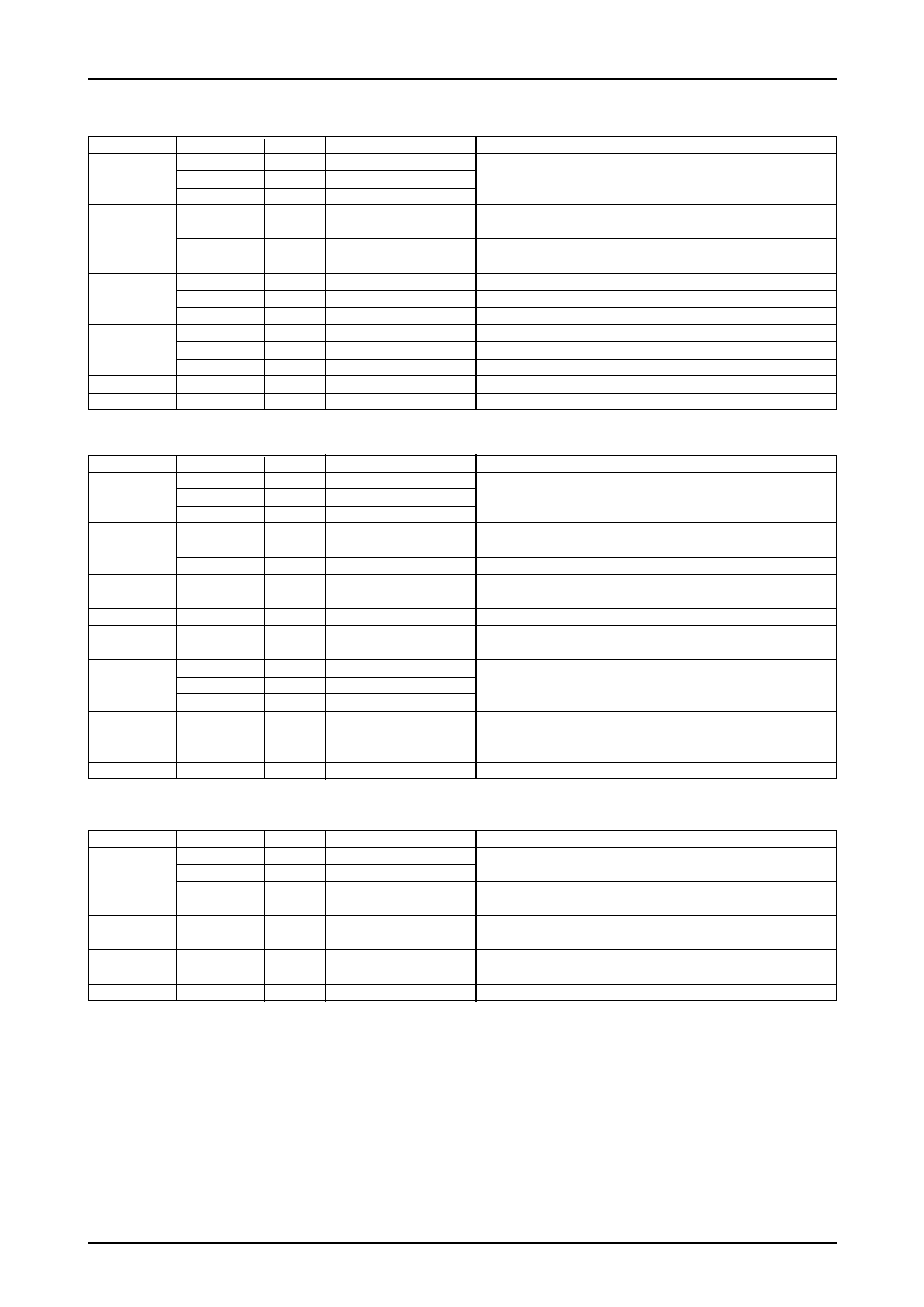
No.8096-5/17
LC749450NW
Signal type
Number of pins
Symbol
Description
Notes
Video signals
10
YIN
Y or G
NTSC/PAL/DTV (4801, 480P, 1080I)
10
CBI
Cb or B or C
or progressive scan RGB (up to SXGA)
10
CRI
Cr or R or OSD
or NTSC/PAL decoder input
Sync signals
1
DHS
Horizontal sync signal
Pixel sync horizontal sync signal input
The polarity can be switched by setting the DVPOLIN internal register.
1
DVS
Vertical sync signal
Vertical sync signal input
The polarity can be switched by setting the DVPOLIN internal register.
Data enable
1
DEHI
Data enable
Valid video period enable signal (horizontal/composite)
signals
1
DEVI
Vertical data enable
Valid video period enable signal (vertical)
1
FIELD
Field signal input
Pixel clock
1
CLKI
Clock
System clock input
Fixed oscillator
1
DCLKI
Used for the output dot clock
System clock input
1
XTAL
Fixed clock input or test clock input
System reset
1
XRST
System reset
System reset input, active low
Total
40
—
I/O Specifications
Input Signals
Signal type
Number of pins
Symbol
Description
Notes
Video signals
10
ODG
G
RGB output
10
ODB
B
The LC749450NW also supports dithered 8-bit output.
10
ODR
R
Sync signals
1
DHO
Horizontal sync signal
This pin outputs the DHS pin input after a delay. (Used for pixel sync.)
(This can be set over the I2C bus.)
1
DVO
Vertical sync signal
Outputs a vertical pixel sync signal.
Data enable
1
AREA
Data enable
Outputs a valid area signal.
signals
Pixel clocks
1
CLKOUT
Outputs the input clock
The polarity can be inverted.
Clamp pulse
1
CLAMPO
For A/D conversion
Outputs a pulse signal used for A/D conversion clamp period verification
signals
Clamp levels
1
CLPG
Y/G clamp level
Clamp level discrimination output
1
CLPB
Cb/B clamp level
(Too large: low, too small: high, match: high-impedance)
1
CLPR
Cr/R clamp level
Field
1
ODEVPPO Field discrimination
Outputs an odd/even field discrimination signal
discrimination
(Used when IP conversion is not used.)
signals
Total
39
—
Output Signals
Signal type
Number of pins
Symbol
Description
Notes
I2C bus signals
1
SDAIO
Data bus
Used for setting internal registers and reading out the internal status.
1
SCLI
Bus clock
The slave address is “1110000+(R/W)”.
1
SLADR
Slave switching
Sets the I2C bus slave address.
Normally low, High: E2h, Low: E0h.
Data output
1
OE
Data output enable signal
signals
XTAL
1
XTALSW
This signal sets the XTAL clock pin input operation
High: The XTAL clock input signal is divided by 2.
Total
5
—
Control Signals
相關PDF資料 |
PDF描述 |
|---|---|
| LC749460W | SPECIALTY CONSUMER CIRCUIT, PQFP256 |
| LC749460W | SPECIALTY CONSUMER CIRCUIT, PQFP256 |
| LC74950BG | SPECIALTY CONSUMER CIRCUIT, PBGA96 |
| LC74950BG | SPECIALTY CONSUMER CIRCUIT, PBGA96 |
| LC74980W | SPECIALTY CONSUMER CIRCUIT, PQFP208 |
相關代理商/技術參數 |
參數描述 |
|---|---|
| LC749460W | 制造商:SANYO 制造商全稱:Sanyo Semicon Device 功能描述:Silicon gate Digital RGB Processor LSI |
| LC74950BG | 制造商:SANYO 制造商全稱:Sanyo Semicon Device 功能描述:CMOS IC Silicon gate 40/30MSPS Analog Display I/F LSI |
| LC74950BG-TLM-H | 功能描述:視頻模擬/數字化轉換器集成電路 RoHS:否 制造商:Texas Instruments 輸入信號類型:Differential 轉換器數量:1 ADC 輸入端數量:4 轉換速率:3 Gbps 分辨率:8 bit 結構: 輸入電壓:3.3 V 接口類型:SPI 信噪比: 電壓參考: 電源電壓-最大:3.45 V 電源電壓-最小:3.15 V 最大功率耗散: 最大工作溫度:+ 85 C 最小工作溫度:- 40 C 封裝 / 箱體:TCSP-48 封裝:Reel |
| LC74980W | 制造商:未知廠家 制造商全稱:未知廠家 功能描述: |
| LC74981W | 制造商:未知廠家 制造商全稱:未知廠家 功能描述: |
發布緊急采購,3分鐘左右您將得到回復。