- 您現在的位置:買賣IC網 > PDF目錄30734 > LC74950BG SPECIALTY CONSUMER CIRCUIT, PBGA96 PDF資料下載
參數資料
| 型號: | LC74950BG |
| 元件分類: | 消費家電 |
| 英文描述: | SPECIALTY CONSUMER CIRCUIT, PBGA96 |
| 封裝: | 6 X 6 MM, FBGA-96 |
| 文件頁數: | 12/37頁 |
| 文件大小: | 350K |
| 代理商: | LC74950BG |
第1頁第2頁第3頁第4頁第5頁第6頁第7頁第8頁第9頁第10頁第11頁當前第12頁第13頁第14頁第15頁第16頁第17頁第18頁第19頁第20頁第21頁第22頁第23頁第24頁第25頁第26頁第27頁第28頁第29頁第30頁第31頁第32頁第33頁第34頁第35頁第36頁第37頁
LC74950BG
No.A1647-2/37
Functions & Overview
1. Input
All the inputs listed below can be connected to the analog ports. It is also possible to switch between the inputs of
two systems and use the one selected.
YCbCr/YPbPr input (480I/576I, 480P/576P): Component input
RGB: RGB input
External clock supported
2. Output
Digital 8-bit/channel output
3. Clamp
Analog clamping and digital clamping supported
4. Gain
Digital gain adjustment
5. PLL circuit
This circuit can be used as the H lock or frequency-multiplied clock. It is also possible to use the PLL circuit and
analog-digital converter (ADC) independently.
H lock PLL circuit: This makes it possible to generate a clock synchronized with the external H sync signal.
Frequency-multiplier PLL circuit: This makes it possible to generate clocks synchronized with an external clock.
6. External interface
I
2C: This supports the 100kHz mode. It is possible to select slave addresses by establishing pin settings.
Slave addresses: 0x98, 0x9A
7. PDOWN
Power-down of the whole system can be controlled using the PDOWN pin. Alternatively, the ADC, PLL and other
circuits can be powered down separately using register settings. This makes it possible to limit the power as required.
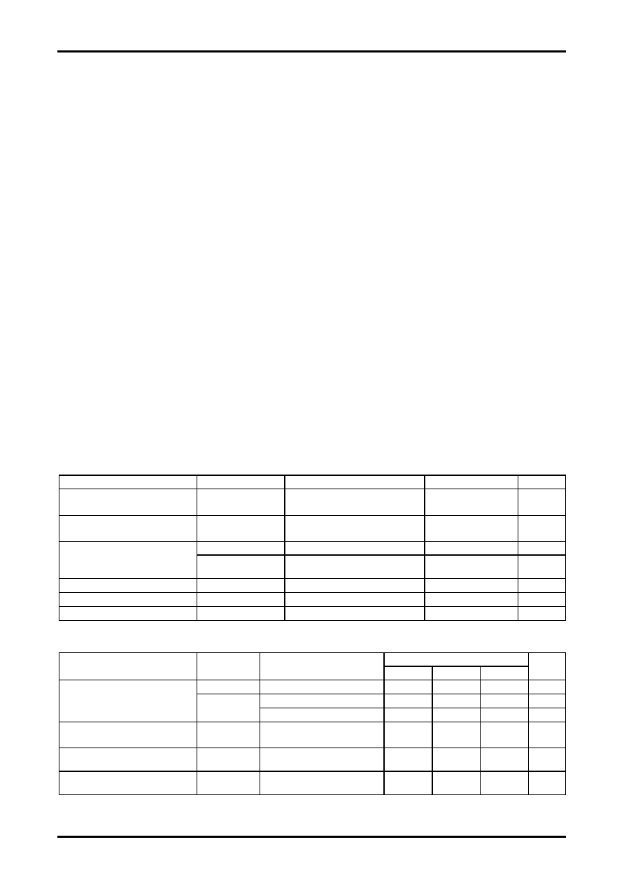
Specifications
Absolute Maximum Ratings at Ta = 25
°C, DVSS = 0V, AVSS = 0V
Parameter
Symbol
Conditions
Ratings
Unit
Maximum supply voltage (I/O)
DVDD33
AVDD33
-0.3 to +3.95
V
Maximum supply voltage (core)
DVDD15
AVDD15
-0.3 to +1.8
V
VI
-0.3 to +5.5
V
Digital input voltage
VI
(when in low voltage)
-0.3 to DVDD33+0.3
V
Digital output voltage
VO
-0.3 to DVDD33+0.3
V
Operating temperature
Topr
-30 to +70
°C
Storage temperature
Tstg
-55 to +125
°C
Allowable Operating Ranges at Ta = -30 to +70
°C
Ratings
Parameter
Symbol
Conditions
min
typ
max
unit
AVDD33
3.00
3.3
3.60
V
Max 40MHz
3.00
3.3
3.60
V
Supply voltage (I/O)
DVDD33
Max 30MHz
2.40
3.3
3.60
V
Supply voltage (I/O)
DVDD15
AVDD15
1.35
1.5
1.65
V
Input voltage range
(5V withstand voltage pin)
VIN5
0
5.5
V
Input voltage range
(non-5V withstand voltage pin)
VIN
0
3.9
V
相關PDF資料 |
PDF描述 |
|---|---|
| LC74980W | SPECIALTY CONSUMER CIRCUIT, PQFP208 |
| LC74981W | SPECIALTY CONSUMER CIRCUIT, PQFP208 |
| LC74982W | SPECIALTY CONSUMER CIRCUIT, PQFP208 |
| LC74986NW-XXXXF | SPECIALTY CONSUMER CIRCUIT, PQFP144 |
| LC74986NW-XXXXV | SPECIALTY CONSUMER CIRCUIT, PQFP144 |
相關代理商/技術參數 |
參數描述 |
|---|---|
| LC74950BG-TLM-H | 功能描述:視頻模擬/數字化轉換器集成電路 RoHS:否 制造商:Texas Instruments 輸入信號類型:Differential 轉換器數量:1 ADC 輸入端數量:4 轉換速率:3 Gbps 分辨率:8 bit 結構: 輸入電壓:3.3 V 接口類型:SPI 信噪比: 電壓參考: 電源電壓-最大:3.45 V 電源電壓-最小:3.15 V 最大功率耗散: 最大工作溫度:+ 85 C 最小工作溫度:- 40 C 封裝 / 箱體:TCSP-48 封裝:Reel |
| LC74980W | 制造商:未知廠家 制造商全稱:未知廠家 功能描述: |
| LC74981W | 制造商:未知廠家 制造商全稱:未知廠家 功能描述: |
| LC74982W | 制造商:SANYO 制造商全稱:Sanyo Semicon Device 功能描述:LCD TV Scan Converter IC |
| LC749870W | 制造商:SANYO 制造商全稱:Sanyo Semicon Device 功能描述:Silicon gate NTSC/PAL/SECAM Digital Video Decoder |
發布緊急采購,3分鐘左右您將得到回復。