- 您現在的位置:買賣IC網 > PDF目錄30734 > LC74950BG SPECIALTY CONSUMER CIRCUIT, PBGA96 PDF資料下載
參數資料
| 型號: | LC74950BG |
| 元件分類: | 消費家電 |
| 英文描述: | SPECIALTY CONSUMER CIRCUIT, PBGA96 |
| 封裝: | 6 X 6 MM, FBGA-96 |
| 文件頁數: | 8/37頁 |
| 文件大小: | 350K |
| 代理商: | LC74950BG |
第1頁第2頁第3頁第4頁第5頁第6頁第7頁當前第8頁第9頁第10頁第11頁第12頁第13頁第14頁第15頁第16頁第17頁第18頁第19頁第20頁第21頁第22頁第23頁第24頁第25頁第26頁第27頁第28頁第29頁第30頁第31頁第32頁第33頁第34頁第35頁第36頁第37頁
LC74950BG
No.A1647-16/37
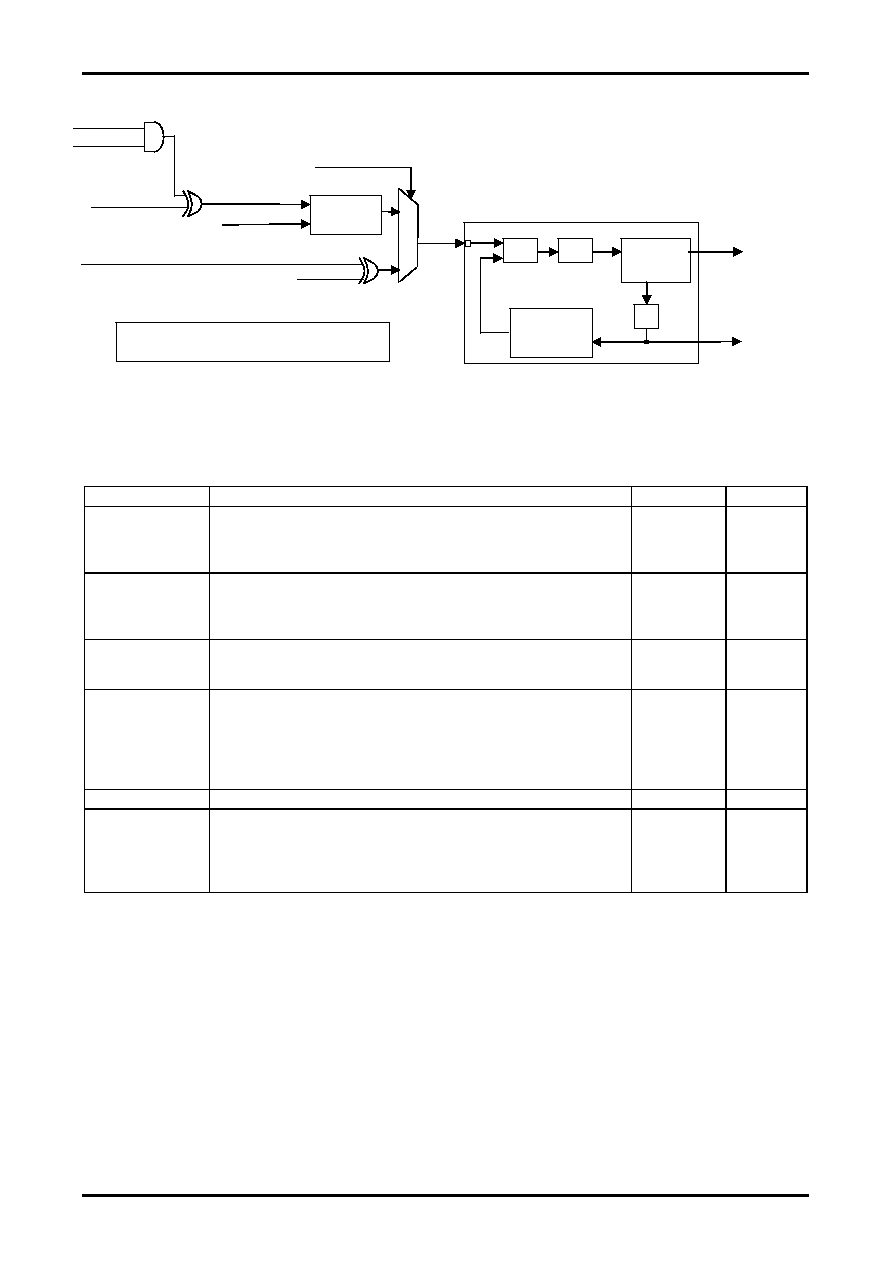
2) PLL circuit
This circuit can be used as the H lock or frequency-multiplied clock. It is also possible to use the PLL circuit and
analog-digital converter (ADC) independently.
H lock PLL circuit: This makes it possible to generate a clock that is synchronized with the external H sync signal.
Frequency-multiplier PLL circuit: This makes it possible to generate clocks that are synchronized with an external clock.
Registers related to the setting of PLL circuit
Name
Functions
Sub address
bit width
CLKININV
This register controls the inversion of CLKIN when the CLKIN input is used as a
reference clock to PLL.
0: Uses CLKIN in its original form
1: Uses CLKIN in its inverted form
0x00
2
HSINV
This register controls the inversion of HSIN input. The HSIN must be used in its
inverted form when the polarity of HSIN input is negative.
0: Original form (when HSIN is positive)
1: Inverted form (when HSIN is negative)
0x02
1
CLKINDIV
This register sets the frequency division ratio of CLKIN to an arbitrary value
(1/1 to 1/64) when the CLKIN is used as a reference clock to PLL.
1/(CLKINDIV[5:0] 1) division
0x40
6
CLKSEL
This register selects the PLL reference input.
000: L fixed (PLL not used)
001: External clock input (CLKIN)
010: External Hsync input (HSIN)
011: External clock input (CLKIN)
100: External clock input (CLKIN)
0x00
3
HPLDIV15-12
This register sets the output divider (M-1, NTSC, 480i=3).
0x28
4
HPLDIV11-0
This register sets the feedback divider (N-2, NTSC, 480i=856).
H-lock PLL output frequency (1x)=Hsync frequency
×N
H-lock PLL output frequency (2x)=Hsync frequency
×N×2
* After changing the setting, an interval of 3.0ms is required for the H-lock PLL to get
stabilized.
0x28
0x29
12
Continued on next page.
FIN
PLL
VCO
Output
Divider
(M=1 to 16)
FOUT
×2
Feedback
Divider
(N=2 to 4097)
1/2
FOUT
CLKIN
POWERIN
CLKINDIV
CLKSEL
40h, bit5-0
00h, bit4
CLKININV
00h, bit2-0
03h, bit3
HSINV
/
6
1/1 to 1/64
Divider
HSIN
FOUTX2 frequency=(FIN frequency)
×M×2×N
FOUT frequency=(FIN frequency)
×M×N
相關PDF資料 |
PDF描述 |
|---|---|
| LC74980W | SPECIALTY CONSUMER CIRCUIT, PQFP208 |
| LC74981W | SPECIALTY CONSUMER CIRCUIT, PQFP208 |
| LC74982W | SPECIALTY CONSUMER CIRCUIT, PQFP208 |
| LC74986NW-XXXXF | SPECIALTY CONSUMER CIRCUIT, PQFP144 |
| LC74986NW-XXXXV | SPECIALTY CONSUMER CIRCUIT, PQFP144 |
相關代理商/技術參數 |
參數描述 |
|---|---|
| LC74950BG-TLM-H | 功能描述:視頻模擬/數字化轉換器集成電路 RoHS:否 制造商:Texas Instruments 輸入信號類型:Differential 轉換器數量:1 ADC 輸入端數量:4 轉換速率:3 Gbps 分辨率:8 bit 結構: 輸入電壓:3.3 V 接口類型:SPI 信噪比: 電壓參考: 電源電壓-最大:3.45 V 電源電壓-最小:3.15 V 最大功率耗散: 最大工作溫度:+ 85 C 最小工作溫度:- 40 C 封裝 / 箱體:TCSP-48 封裝:Reel |
| LC74980W | 制造商:未知廠家 制造商全稱:未知廠家 功能描述: |
| LC74981W | 制造商:未知廠家 制造商全稱:未知廠家 功能描述: |
| LC74982W | 制造商:SANYO 制造商全稱:Sanyo Semicon Device 功能描述:LCD TV Scan Converter IC |
| LC749870W | 制造商:SANYO 制造商全稱:Sanyo Semicon Device 功能描述:Silicon gate NTSC/PAL/SECAM Digital Video Decoder |
發布緊急采購,3分鐘左右您將得到回復。