- 您現(xiàn)在的位置:買賣IC網(wǎng) > PDF目錄30735 > LC75386NE 2 CHANNEL(S), TONE CONTROL CIRCUIT, PQFP64 PDF資料下載
參數(shù)資料
| 型號: | LC75386NE |
| 元件分類: | 音頻控制 |
| 英文描述: | 2 CHANNEL(S), TONE CONTROL CIRCUIT, PQFP64 |
| 封裝: | QFP-64 |
| 文件頁數(shù): | 10/20頁 |
| 文件大小: | 319K |
| 代理商: | LC75386NE |
Usage Notes
Notes on data transfer when power is first applied
— The states of the internal analog switches are undefined when power is first applied. Until the control data has been
set up, applications must mute signals appropriately.
— Applications should send initial setup data to quickly stabilize the bias levels in each block when power is first
applied.
The period between initial setup mode and initial data setup
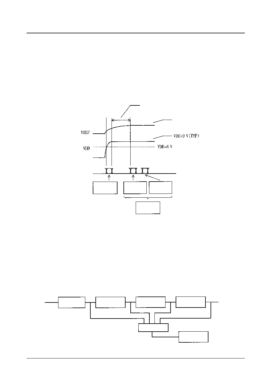
— Applications should transfer the initial setup data after the power-supply voltage VDD exceeds 6 V.
— Send initial data (that turns the rapid charging switches off) after the LCOM, RCOM, and VREF pin levels have
stabilized.
Procedure for transferring the initial setup data
Quick charge mode is set up when D32 and D33 are set to 00. Since the other data (D0 to D31, and D34 to D43) is set
up for the left and right channels at the same time, the states of the other blocks can be set at the same time.
Procedure for clearing the initial setup data
Quick charge mode is cleared when D32 and D33 are set to a value other than 00, that is when normal left/right channel
operation is specified.
Operating Principles of the Zero Cross Switching Circuit
The LC75386NE provides a function that switches the signal detection location of the zero cross comparator. This means
an optimal location for block for data update can be selected. Basically, switching noise can be minimized by inputting
the signal from immediately after the block that modifies the data to the zero cross comparator. Therefore, the detection
location needs to be changed each time the IC control settings are changed.
Zero Cross Detection Circuit
No. 5937-18/20
LC75386NE
Time until the capacitors connected to the LCOM and RCOM
pins are charged to the VREF level.
1/2 VDD level
Initial setup
mode
Data
Initial data
(left channel)
Initial data
(right channel)
These operations
clear initial setup
mode
Selector
Volume
Tone
Fader
Switch
Zero cross comparator
相關(guān)PDF資料 |
PDF描述 |
|---|---|
| LC7538JM | 2 CHANNEL(S), TONE CONTROL CIRCUIT, PDSO36 |
| LC7538NM | 2 CHANNEL(S), TONE CONTROL CIRCUIT, PDSO36 |
| LC75391 | 2 CHANNEL(S), TONE CONTROL CIRCUIT, PDIP30 |
| LC75391M | 2 CHANNEL(S), TONE CONTROL CIRCUIT, PDSO30 |
| LC75394E | 2 CHANNEL(S), VOLUME CONTROL CIRCUIT, PQFP64 |
相關(guān)代理商/技術(shù)參數(shù) |
參數(shù)描述 |
|---|---|
| LC75386NE-L | 制造商:SANYO Semiconductor Co Ltd 功能描述:2 CHANNEL(S), TONE CONTROL CIRCUIT, PQFP64 |
| LC75386NE-R | 制造商:SANYO 制造商全稱:Sanyo Semicon Device 功能描述:LC75386NE-R/LC75386NW |
| LC75386NE-R-E | 制造商:ON Semiconductor 功能描述: |
| LC75386NW | 制造商:SANYO 制造商全稱:Sanyo Semicon Device 功能描述:LC75386NE-R/LC75386NW |
| LC7538JM | 制造商:SANYO 制造商全稱:Sanyo Semicon Device 功能描述:Electronic Volume Control System for Car Audio |
發(fā)布緊急采購,3分鐘左右您將得到回復(fù)。