- 您現在的位置:買賣IC網 > PDF目錄30745 > LM2422TE/NOPB (NATIONAL SEMICONDUCTOR CORP) 1 CHANNEL, VIDEO AMPLIFIER, PZFM11 PDF資料下載
參數資料
| 型號: | LM2422TE/NOPB |
| 廠商: | NATIONAL SEMICONDUCTOR CORP |
| 元件分類: | 音頻/視頻放大 |
| 英文描述: | 1 CHANNEL, VIDEO AMPLIFIER, PZFM11 |
| 封裝: | PLASTIC, TO-220, 11 PIN |
| 文件頁數: | 2/8頁 |
| 文件大小: | 604K |
| 代理商: | LM2422TE/NOPB |
Absolute Maximum Ratings (Notes 1,
If Military/Aerospace specified devices are required,
please contact the National Semiconductor Sales Office/
Distributors for availability and specifications.
Supply Voltage (V
CC)
+250V
Bias Voltage (V
BB)
+16V
Input Voltage (V
IN)
0.5V to V
BB +0.5V
Storage Temperature Range (T
STG)
65C to +150C
Lead Temperature
(Soldering, <10 sec.)
300C
ESD Tolerance,
Human Body Model
2 kV
Machine Model
200V
Junction Temperature
150C
θ
JC (typ)
1.8C/W
Operating Ratings (Note 2)
V
CC
+100V to +230V
V
BB
+7V to +13V
V
IN
+0V to +5V
V
OUT
+40V to +215V
Case Temperature
(22W max power)
110C
Do not operate the part without a heat sink. Heat sink
must have a thermal resistance under 2.3C/W. (Note 7)
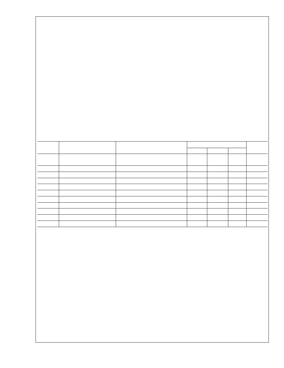
Electrical Characteristics
(See Figure 3 for Test Circuit). Unless otherwise noted: V
CC = +220V, VBB = +12V, CL = 10 pF, TC = 60C. DC Tests: VIN =
+2.7V
DC. AC Tests: Output = 110VPP (80V – 190V) at 1 MHz.
Symbol
Parameter
Conditions
LM2422
Units
Min
Typ
Max
I
CC
Supply Current
No Input Signal, No Video Input, No
Output Load
36
45
54
mA
I
BB
Bias Current
18
27
36
mA
V
OUT, 1
DC Output Voltage
No AC Input Signal, V
IN = 2.7VDC
124
129
134
V
DC
V
OUT, 2
DC Output Voltage
No AC Input Signal, V
IN = 1.2VDC
200
205
210
V
DC
A
V
DC Voltage Gain
No AC Input Signal
49
52
55
V/V
A
V
Gain Matching
(Note 4), No AC Input Signal
1.0
dB
LE
Linearity Error
(Notes 4, 5), No AC Input Signal
8
%
t
r
Rise Time, 80V to 190V
(Note 6), 10% to 90%
12
ns
+OS
Overshoot
12
%
t
f
Fall Time, 80V to 190V
(Note 6), 90% to 10%
12
ns
OS
Overshoot
4
%
Note 1: Absolute Maximum Ratings indicate limits beyond which damage to the device may occur.
Note 2: Operating ratings indicate conditions for which the device is functional, but do not guarantee specific performance limits. For guaranteed specifications and
test conditions, see the Electrical Characteristics. Datasheet min/max specification limits are guaranteed by design, test, or statistical analysis. The guaranteed
specifications apply only for the test conditions listed. Some performance characteristics may change when the device is not operated under the listed test
conditions.
Note 3: All voltages are measured with respect to GND, unless otherwise specified.
Note 4: Calculated value from Voltage Gain test on each channel.
Note 5: Linearity Error is the variation in DC gain from VIN = 1.15V to VIN = 4.35V.
Note 6: Input from signal generator: tr,tf < 1 ns.
Note 7: Running the 1 MHz to 30 MHz test pattern at 1080i this part will dissipate approximately 22 W. This is the commonly accepted test pattern that is
representative of the worst case high frequency content for normal television viewing. This is the pattern used to estimate the worst case power dissipation of the
LM2422 in its normal application. It is recommended to use a heat sink with a thermal resistance of 2.3C/W or better.
LM2422
www.national.com
2
相關PDF資料 |
PDF描述 |
|---|---|
| LM2423TE/NOPB | 1 CHANNEL, VIDEO AMPLIFIER, PZFM11 |
| LM2426TA | 3 CHANNEL, VIDEO AMPLIFIER, PZFM11 |
| LM2433TE | 1 CHANNEL, VIDEO AMPLIFIER, PSFM7 |
| LM2436TA/NOPB | 3 CHANNEL, VIDEO AMPLIFIER, PZFM9 |
| LM2457TA | 3 CHANNEL, VIDEO AMPLIFIER, PZFM15 |
相關代理商/技術參數 |
參數描述 |
|---|---|
| LM2423 | 制造商:NSC 制造商全稱:National Semiconductor 功能描述:220V Monolithic Triple Channel 15 MHz CRT DTV Driver |
| LM2423_06 | 制造商:NSC 制造商全稱:National Semiconductor 功能描述:220V Monolithic Triple Channel 15 MHz CRT DTV Driver |
| LM2423TE | 制造商:Texas Instruments 功能描述:IC,TV/VIDEO CIRCUIT,Driver,BIPOLAR,ZIP,11PIN,PLASTIC |
| LM2423TE/NOPB | 功能描述:顯示驅動器和控制器 RoHS:否 制造商:Panasonic Electronic Components 工作電源電壓:2.7 V to 5.5 V 最大工作溫度: 安裝風格:SMD/SMT 封裝 / 箱體:QFN-44 封裝:Reel |
| LM2425 | 制造商:NSC 制造商全稱:National Semiconductor 功能描述:220V Monolithic Triple Channel 10 MHz CRT DTV Driver |
發布緊急采購,3分鐘左右您將得到回復。