- 您現(xiàn)在的位置:買賣IC網(wǎng) > PDF目錄361030 > LM5642MTC (NATIONAL SEMICONDUCTOR CORP) High Voltage, Dual Synchronous Buck Converter with Oscillator Synchronization PDF資料下載
參數(shù)資料
| 型號(hào): | LM5642MTC |
| 廠商: | NATIONAL SEMICONDUCTOR CORP |
| 元件分類: | 穩(wěn)壓器 |
| 英文描述: | High Voltage, Dual Synchronous Buck Converter with Oscillator Synchronization |
| 中文描述: | DUAL SWITCHING CONTROLLER, 226 kHz SWITCHING FREQ-MAX, PDSO28 |
| 封裝: | TSSOP-28 |
| 文件頁(yè)數(shù): | 2/24頁(yè) |
| 文件大小: | 667K |
| 代理商: | LM5642MTC |
第1頁(yè)當(dāng)前第2頁(yè)第3頁(yè)第4頁(yè)第5頁(yè)第6頁(yè)第7頁(yè)第8頁(yè)第9頁(yè)第10頁(yè)第11頁(yè)第12頁(yè)第13頁(yè)第14頁(yè)第15頁(yè)第16頁(yè)第17頁(yè)第18頁(yè)第19頁(yè)第20頁(yè)第21頁(yè)第22頁(yè)第23頁(yè)第24頁(yè)
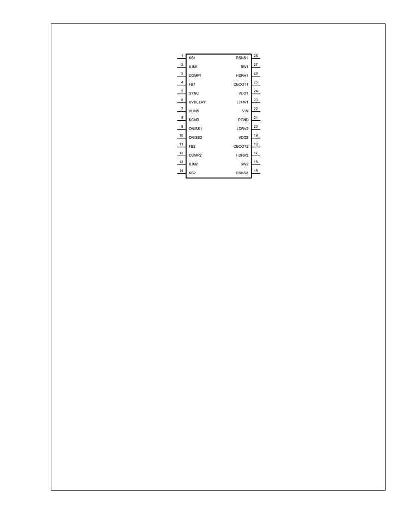
Connection Diagram
TOP VIEW
20060102
28-Lead TSSOP (MTC)
Order Number LM5642MTC
See NS Package Number MTC28
Pin Descriptions
KS1 (Pin 1):
The positive (+) Kelvin sense for the internal
current sense amplifier of Channel 1. Use a separate trace to
connect this pin to the current sense point. It should be
connected to VIN as close as possible to the node of the
current sense resistor. When no current-sense resistor is
used, connect as close as possible to the drain node of the
upper MOSFET.
ILIM1 (Pin 2):
Current limit threshold setting for Channel 1. It
sinks a constant current of 9.9μA, which is converted to a
voltage across a resistor connected from this pin to VIN. The
voltage across the resistor is compared with either the V
of the top MOSFET or the voltage across the external cur-
rent sense resistor to determine if an over-current condition
has occurred in Channel 1.
COMP1 (Pin 3):
Compensation pin for Channel 1. This is the
output of the internal transconductance amplifier. The com-
pensation network should be connected between this pin
and the signal ground, SGND (Pin 8).
FB1 (Pin 4):
Feedback input for channel 1. Connect to
VOUT through a voltage divider to set the Channel 1 output
voltage.
SYNC (Pin 5):
The switching frequency of the LM5642 can
be synchronized to an external clock.
SYNC = LOW:
Free running at 200kHz, channels are 180
out of phase.
SYNC = HIGH:
Waiting for external clock
SYNC = Falling Edge:
Channel 1 HDRV pin goes high.
Channel 2 HDRV pin goes high after 2.5μs delay. The maxi-
mum SYNC pulse width must be greater than 100ns.
For SYNC = Low operation, connect this pin to signal ground
through a 220k
resistor.
UV_DELAY (Pin 6):
A capacitor from this pin to ground sets
the delay time for UVP. The capacitor is charged from a 5μA
current source. When UV_DELAY charges to 2.3V (typical),
the system immediately latches off. Connecting this pin to
ground will disable the output under-voltage protection.
VLIN5 (Pin 7):
The output of an internal 5V LDO regulator
derived from VIN. It supplies the internal bias for the chip and
supplies the bootstrap circuitry for gate drive. Bypass this pin
to signal ground with a minimum of 4.7μF ceramic capacitor.
SGND (Pin 8):
The ground connection for the signal-level
circuitry. It should be connected to the ground rail of the
system.
ON/SS1 (Pin 9):
Channel 1 enable pin. This pin is internally
pulled up to one diode drop above VLIN5. Pulling this pin
below 1.2V (open-collector type) turns off Channel 1. If both
ON/SS1 and ON/SS2 pins are pulled below 1.2V, the whole
chip goes into
shut down mode
. Adding a capacitor to this
pin provides a soft-start feature that minimizes inrush current
and output voltage overshoot.
ON/SS2 (Pin 10):
Channel 2 enable pin. See the description
for Pin 9, ON/SS1. May be connected to ON/SS1 for simul-
taneous startup or for parallel operation.
FB2 (Pin 11):
Feedback input for channel 2. Connect to
VOUT through a voltage divider to set the Channel 2 output
voltage.
COMP2 (Pin 12):
Compensation pin for Channel 2. This is
the output of the internal transconductance amplifier. The
compensation network should be connected between this
pin and the signal ground SGND (Pin 8).
ILIM2 (Pin 13):
Current limit threshold setting for Channel 2.
See ILIM1 (Pin 2).
KS2 (Pin 14):
The positive (+) Kelvin sense for the internal
current sense amplifier of Channel 2. See KS1 (Pin 1).
RSNS2 (Pin 15):
The negative (-) Kelvin sense for the
internal current sense amplifier of Channel 2. Connect this
pin to the low side of the current sense resistor that is placed
between VIN and the drain of the top MOSFET. When the
L
www.national.com
2
相關(guān)PDF資料 |
PDF描述 |
|---|---|
| LM565 | Phase Locked Loop |
| LM565C | |
| LM565CH | Analog Phase-Locked Loop |
| LM565CN | Phase Locked Loop |
| LM565H | CAP 63V 330UF ELECT AXIAL |
相關(guān)代理商/技術(shù)參數(shù) |
參數(shù)描述 |
|---|---|
| LM5642MTC/NOPB | 功能描述:DC/DC 開關(guān)控制器 RoHS:否 制造商:Texas Instruments 輸入電壓:6 V to 100 V 開關(guān)頻率: 輸出電壓:1.215 V to 80 V 輸出電流:3.5 A 輸出端數(shù)量:1 最大工作溫度:+ 125 C 安裝風(fēng)格: 封裝 / 箱體:CPAK |
| LM5642MTCX | 功能描述:DC/DC 開關(guān)控制器 RoHS:否 制造商:Texas Instruments 輸入電壓:6 V to 100 V 開關(guān)頻率: 輸出電壓:1.215 V to 80 V 輸出電流:3.5 A 輸出端數(shù)量:1 最大工作溫度:+ 125 C 安裝風(fēng)格: 封裝 / 箱體:CPAK |
| LM5642MTCX/NOPB | 功能描述:DC/DC 開關(guān)控制器 RoHS:否 制造商:Texas Instruments 輸入電壓:6 V to 100 V 開關(guān)頻率: 輸出電壓:1.215 V to 80 V 輸出電流:3.5 A 輸出端數(shù)量:1 最大工作溫度:+ 125 C 安裝風(fēng)格: 封裝 / 箱體:CPAK |
| LM5642XMH | 功能描述:DC/DC 開關(guān)控制器 RoHS:否 制造商:Texas Instruments 輸入電壓:6 V to 100 V 開關(guān)頻率: 輸出電壓:1.215 V to 80 V 輸出電流:3.5 A 輸出端數(shù)量:1 最大工作溫度:+ 125 C 安裝風(fēng)格: 封裝 / 箱體:CPAK |
| LM5642XMH/NOPB | 功能描述:DC/DC 開關(guān)控制器 RoHS:否 制造商:Texas Instruments 輸入電壓:6 V to 100 V 開關(guān)頻率: 輸出電壓:1.215 V to 80 V 輸出電流:3.5 A 輸出端數(shù)量:1 最大工作溫度:+ 125 C 安裝風(fēng)格: 封裝 / 箱體:CPAK |
發(fā)布緊急采購(gòu),3分鐘左右您將得到回復(fù)。