- 您現(xiàn)在的位置:買(mǎi)賣(mài)IC網(wǎng) > PDF目錄361030 > LM5642MTC (NATIONAL SEMICONDUCTOR CORP) High Voltage, Dual Synchronous Buck Converter with Oscillator Synchronization PDF資料下載
參數(shù)資料
| 型號(hào): | LM5642MTC |
| 廠商: | NATIONAL SEMICONDUCTOR CORP |
| 元件分類(lèi): | 穩(wěn)壓器 |
| 英文描述: | High Voltage, Dual Synchronous Buck Converter with Oscillator Synchronization |
| 中文描述: | DUAL SWITCHING CONTROLLER, 226 kHz SWITCHING FREQ-MAX, PDSO28 |
| 封裝: | TSSOP-28 |
| 文件頁(yè)數(shù): | 20/24頁(yè) |
| 文件大小: | 667K |
| 代理商: | LM5642MTC |
第1頁(yè)第2頁(yè)第3頁(yè)第4頁(yè)第5頁(yè)第6頁(yè)第7頁(yè)第8頁(yè)第9頁(yè)第10頁(yè)第11頁(yè)第12頁(yè)第13頁(yè)第14頁(yè)第15頁(yè)第16頁(yè)第17頁(yè)第18頁(yè)第19頁(yè)當(dāng)前第20頁(yè)第21頁(yè)第22頁(yè)第23頁(yè)第24頁(yè)
Input Capacitor Selection
(Continued)
3.
Both duty cycles are greater than D
MAX
. This case is
identical to a system at 200kHz where either duty cycle
is 50% or greater. Some overlap of duty cycles is guar-
anteed, and hence the second, more complicated rms
input current equation must be used.
Input capacitors must meet the minimum requirements of
voltage and ripple current capacity. The size of the capacitor
should then be selected based on hold up time require-
ments. Bench testing for individual applications is still the
best way to determine a reliable input capacitor value. Input
capacitors should always be placed as close as possible to
the current sense resistor or the drain of the top FET. When
high ESR capacitors such as tantalum are used, a 1μF
ceramic capacitor should be added as closely as possible to
the high-side FET drain and low-side FET source.
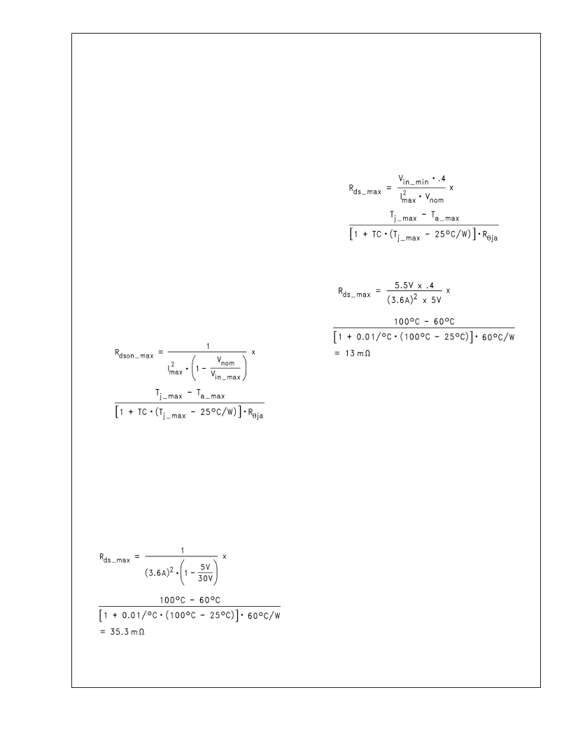
MOSFET Selection
BOTTOM FET SELECTION
During normal operation, the bottom FET is switching on and
off at almost zero voltage. Therefore, only conduction losses
are present in the bottom FET. The most important param-
eter when selecting the bottom FET is the on resistance
(R
DS-ON
). The lower the on resistance, the lower the power
loss. The bottom FET power loss peaks at maximum input
voltage and load current. The equation for the maximum
allowed on resistance at room temperature for a given FET
package, is:
(25)
where Tj_max is the maximum allowed junction temperature
in the FET, Ta_max is the maximum ambient temperature,
R
θ
ja
is the junction-to-ambient thermal resistance of the FET,
and TC is the temperature coefficient of the on resistance
which is typically in the range of 10,000ppm/C.
If the calculated R
DS-ON (MAX)
is smaller than the lowest
value available, multiple FETs can be used in parallel. This
effectively reduces the Imax term in the above equation, thus
reducing R
. When using two FETs in parallel, multiply
the calculated R
by 4 to obtain the R
for each FET. In the case of three FETs, multiply by 9.
(26)
If the selected FET has an Rds value higher than 35.3
,
then two FETs with an R
DS-ON
less than 141m
(4 x
35.3m
) can be used in parallel. In this case, the tempera-
ture rise on each FET will not go to Tj_max because each
FET is now dissipating only half of the total power.
TOP FET SELECTION
The top FET has two types of losses: switching loss and
conduction loss. The switching losses mainly consist of
crossover loss and bottom diode reverse recovery loss.
Since it is rather difficult to estimate the switching loss, a
general starting point is to allot 60% of the top FET thermal
capacity to switching losses. The best way to precisely de-
termine switching losses is through bench testing. The equa-
tion for calculating the on resistance of the top FET is thus:
(27)
Example: Tj_max = 100C, Ta_max = 60C, Rqja = 60C/W,
Vin_min = 5.5V, Vnom = 5V, and Iload_max = 3.6A.
(28)
When using FETs in parallel, the same guidelines apply to
the top FET as apply to the bottom FET.
Loop Compensation
The general purpose of loop compensation is to meet static
and dynamic performance requirements while maintaining
stability. Loop gain is what is usually checked to determine
small-signal performance. Loop gain is equal to the product
of control-output transfer function and the output-control
transfer function (the compensation network transfer func-
tion). Generally speaking it is a good idea to have a loop gain
slope that is -20dB /decade from a very low frequency to well
beyond the crossover frequency. The crossover frequency
should not exceed one-fifth of the switching frequency. The
higher the bandwidth is, the faster the load transient re-
sponse speed will potentially be. However, if the duty cycle
saturates during a load transient, further increasing the small
signal bandwidth will not help. Since the control-output trans-
fer function usually has very limited low frequency gain, it is
a good idea to place a pole in the compensation at zero
frequency, so that the low frequency gain will be relatively
large. A large DC gain means high DC regulation accuracy
(i.e. DC voltage changes little with load or line variations).
The rest of the compensation scheme depends highly on the
shape of the control-output plot.
L
www.national.com
20
相關(guān)PDF資料 |
PDF描述 |
|---|---|
| LM565 | Phase Locked Loop |
| LM565C | |
| LM565CH | Analog Phase-Locked Loop |
| LM565CN | Phase Locked Loop |
| LM565H | CAP 63V 330UF ELECT AXIAL |
相關(guān)代理商/技術(shù)參數(shù) |
參數(shù)描述 |
|---|---|
| LM5642MTC/NOPB | 功能描述:DC/DC 開(kāi)關(guān)控制器 RoHS:否 制造商:Texas Instruments 輸入電壓:6 V to 100 V 開(kāi)關(guān)頻率: 輸出電壓:1.215 V to 80 V 輸出電流:3.5 A 輸出端數(shù)量:1 最大工作溫度:+ 125 C 安裝風(fēng)格: 封裝 / 箱體:CPAK |
| LM5642MTCX | 功能描述:DC/DC 開(kāi)關(guān)控制器 RoHS:否 制造商:Texas Instruments 輸入電壓:6 V to 100 V 開(kāi)關(guān)頻率: 輸出電壓:1.215 V to 80 V 輸出電流:3.5 A 輸出端數(shù)量:1 最大工作溫度:+ 125 C 安裝風(fēng)格: 封裝 / 箱體:CPAK |
| LM5642MTCX/NOPB | 功能描述:DC/DC 開(kāi)關(guān)控制器 RoHS:否 制造商:Texas Instruments 輸入電壓:6 V to 100 V 開(kāi)關(guān)頻率: 輸出電壓:1.215 V to 80 V 輸出電流:3.5 A 輸出端數(shù)量:1 最大工作溫度:+ 125 C 安裝風(fēng)格: 封裝 / 箱體:CPAK |
| LM5642XMH | 功能描述:DC/DC 開(kāi)關(guān)控制器 RoHS:否 制造商:Texas Instruments 輸入電壓:6 V to 100 V 開(kāi)關(guān)頻率: 輸出電壓:1.215 V to 80 V 輸出電流:3.5 A 輸出端數(shù)量:1 最大工作溫度:+ 125 C 安裝風(fēng)格: 封裝 / 箱體:CPAK |
| LM5642XMH/NOPB | 功能描述:DC/DC 開(kāi)關(guān)控制器 RoHS:否 制造商:Texas Instruments 輸入電壓:6 V to 100 V 開(kāi)關(guān)頻率: 輸出電壓:1.215 V to 80 V 輸出電流:3.5 A 輸出端數(shù)量:1 最大工作溫度:+ 125 C 安裝風(fēng)格: 封裝 / 箱體:CPAK |
發(fā)布緊急采購(gòu),3分鐘左右您將得到回復(fù)。