- 您現(xiàn)在的位置:買賣IC網(wǎng) > PDF目錄361034 > LM78S40 (National Semiconductor Corporation) RADIATION HARDENED HIGH EFFICIENCY, 5 AMP SWITCHING REGULATORS PDF資料下載
參數(shù)資料
| 型號: | LM78S40 |
| 廠商: | National Semiconductor Corporation |
| 元件分類: | 基準電壓源/電流源 |
| 英文描述: | RADIATION HARDENED HIGH EFFICIENCY, 5 AMP SWITCHING REGULATORS |
| 中文描述: | 抗輻射高效,5安培開關穩(wěn)壓器 |
| 文件頁數(shù): | 3/10頁 |
| 文件大?。?/td> | 289K |
| 代理商: | LM78S40 |
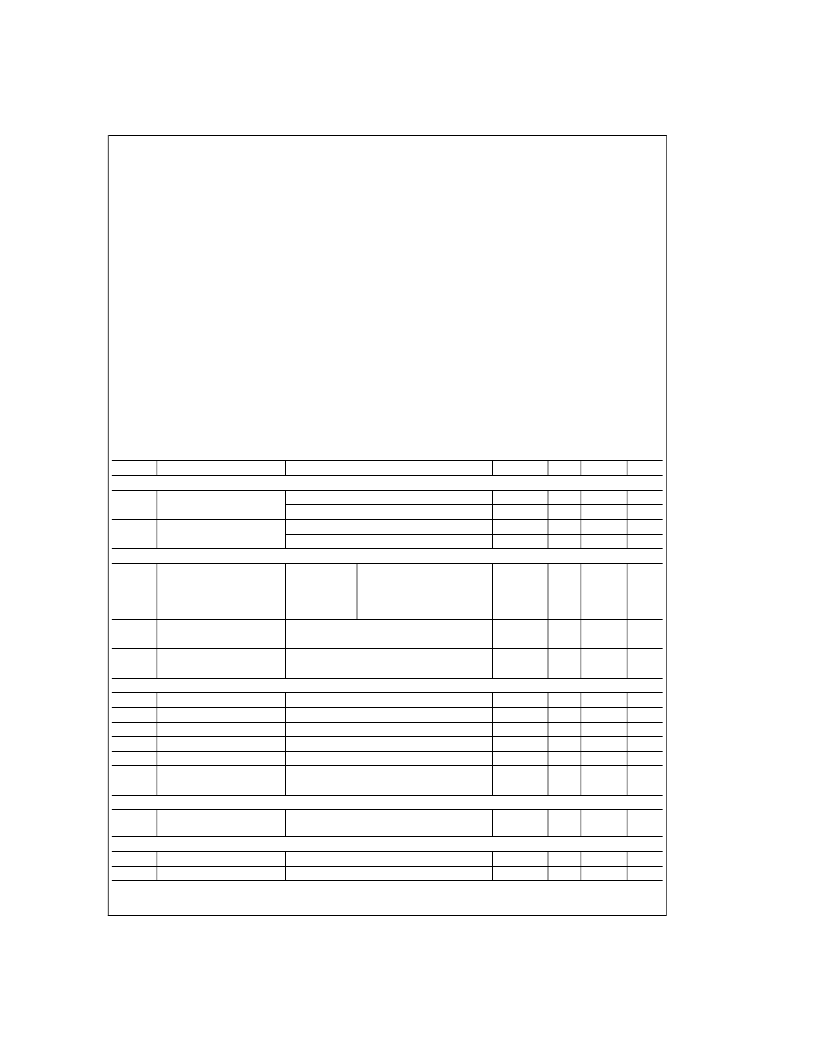
Absolute Maximum Ratings
(Note 1)
If Military/Aerospace specified devices are required,
please contact the National Semiconductor Sales Office/
Distributors for availability and specifications.
Storage Temperature Range
Ceramic DIP
Molded DIP
Operating Temperature Range
Extended (LM78S40J)
Industrial (LM78S40N)
Commercial (LM78S40CN)
Lead Temperature
Ceramic DIP (Soldering, 60 sec.)
Molded DIP (Soldering, 10 sec.)
Internal Power Dissipation (Note 2) (Note 3)
16L-Ceramic DIP
16L-Molded DIP
Input Voltage from V
IN
to GND
Input Voltage from V
+
(Op Amp)
65C to +175C
65C to +150C
55C to +125C
40C to +125C
0C to +70C
300C
265C
1.50W
1.04W
40V
to GND
Common Mode Input Range
(Comparator and Op Amp)
Differential Input Voltage
(Note 4)
Output Short Circuit
Duration (Op Amp)
Current from V
REF
Voltage from Switch
Collectors to GND
Voltage from Switch
Emitters to GND
Voltage from Switch
Collectors to Emitter
Voltage from Power Diode to GND
Reverse Power Diode Voltage
Current through Power Switch
Current through Power Diode
ESD Susceptibility
40V
0.3 to V+
±
30V
Continuous
10 mA
40V
40V
40V
40V
40V
1.5A
1.5A
(to be determined)
LM78S40
Electrical Characteristics
(Note 5)
T
A
= Operating temperature range, V
IN
= 5.0V, V
+
(Op Amp) = 5.0V, unless otherwise specified.
Symbol
Parameter
GENERAL CHARACTERISTICS
I
CC
Supply Current
V
IN
= 5.0V
(Op Amp Disconnected)
V
IN
= 40V
I
CC
Supply Current
V
IN
= 5.0V
(Op Amp Connected)
V
IN
= 40V
REFERENCE SECTION
V
REF
Reference Voltage
I
REF
= 1.0 mA
Conditions
Min
Typ
Max
Units
1.8
2.3
3.5
5.0
4.0
5.5
mA
mA
mA
mA
Extend 55C
<
T
A
<
+125C,
Comm 0
<
T
A
<
+70C,
Indus 40C
<
T
A
<
+85C
1.180
1.245
1.310
V
V
R LINE
Reference Voltage
Line Regulation
Reference Voltage
Load Regulation
V
IN
= 3.0V to V
IN
= 40V,
I
REF
= 1.0 mA, T
A
= 25C
I
REF
= 1.0 mA to I
REF
= 10 mA,
T
A
= 25C
0.04
0.2
mV/V
V
R LOAD
0.2
0.5
mV/mA
OSCILLATOR SECTION
I
CHG
Charging Current
I
CHG
Charging Current
I
DISCHG
Discharge Current
I
DISCHG
Discharge Current
V
OSC
Oscillator Voltage Swing
t
on
/t
off
Ratio of Charge/
Discharge Time
CURRENT LIMIT SECTION
V
CLS
Current Limit Sense
Voltage
OUTPUT SWITCH SECTION
V
SAT 1
Output Saturation Voltage 1
V
SAT 2
Output Saturation Voltage 2
V
IN
= 5.0V, T
A
= 25C
V
IN
= 40V, T
A
= 25C
V
IN
= 5.0V, T
A
= 25C
V
IN
= 40V, T
A
= 25C
V
IN
= 5.0V, T
A
= 25C
20
20
150
150
50
70
250
350
μA
μA
μA
μA
V
μs/μs
0.5
6.0
T
A
= 25C
250
350
mV
I
SW
= 1.0A (Figure 1)
I
SW
= 1.0A (Figure 2)
1.1
0.45
1.3
0.7
V
V
3
www.national.com
相關PDF資料 |
PDF描述 |
|---|---|
| LM78 | Microprocessor System Hardware Monitor |
| LM78CCVF | Microprocessor System Hardware Monitor |
| LM78CCVF-J | Microprocessor System Hardware Monitor |
| LM79CCVF | Microprocessor System Hardware Monitor |
| LM79 | |
相關代理商/技術參數(shù) |
參數(shù)描述 |
|---|---|
| LM78S40CN | 功能描述:直流/直流開關轉(zhuǎn)換器 RoHS:否 制造商:STMicroelectronics 最大輸入電壓:4.5 V 開關頻率:1.5 MHz 輸出電壓:4.6 V 輸出電流:250 mA 輸出端數(shù)量:2 最大工作溫度:+ 85 C 安裝風格:SMD/SMT |
| LM78S40CN | 制造商:Texas Instruments 功能描述:IC SWITCHING REGULATOR |
| LM78S40CN/NOPB | 功能描述:直流/直流開關轉(zhuǎn)換器 Uni Switching Reg Subsystem RoHS:否 制造商:STMicroelectronics 最大輸入電壓:4.5 V 開關頻率:1.5 MHz 輸出電壓:4.6 V 輸出電流:250 mA 輸出端數(shù)量:2 最大工作溫度:+ 85 C 安裝風格:SMD/SMT |
| LM78S40CN/NOPB | 制造商:Texas Instruments 功能描述:DC/DC Converter (DC-DC) / Switching Regu |
| LM78S40J | 制造商:Rochester Electronics LLC 功能描述:- Bulk |
發(fā)布緊急采購,3分鐘左右您將得到回復。