- 您現在的位置:買賣IC網 > PDF目錄361035 > LM9040M (NATIONAL SEMICONDUCTOR CORP) Dual Lambda Sensor Interface Amplifier PDF資料下載
參數資料
| 型號: | LM9040M |
| 廠商: | NATIONAL SEMICONDUCTOR CORP |
| 元件分類: | 測量放大器 |
| 英文描述: | Dual Lambda Sensor Interface Amplifier |
| 中文描述: | DUAL INSTRUMENTATION AMPLIFIER, PDSO14 |
| 封裝: | 0.300 INCH, PLASTIC, SOP-14 |
| 文件頁數: | 4/10頁 |
| 文件大小: | 178K |
| 代理商: | LM9040M |
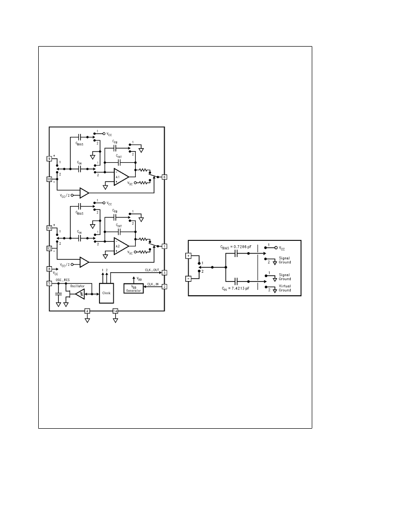
Circuit Description
The LM9040 is fabricated in CMOS technology and is de-
signed to operate from a single, well regulated, 5V supply.
The IC consists of two independent differential amplifiers
which are designed using two-phased switched capacitor
networks (SCN). The differential inputs have a common
mode operating range of 2V above and below ground. The
SCN includes the input sampling, the lowpass filter, cold
sensor bias voltage, and the gain circuitry. Each amplifier
has an independent voltage comparator to detect an open
inverting input pin. Additional support circuitry includes the
oscillator, clock generator, and V
BB
bias generator.
TL/H/12372–13
FIGURE 3. Simplified Circuit
Oscillator
The device contains an internal oscillator which is used to
drive the internal two-phase clock generator. The oscillator
requires an external resistor value of 178 k
X
from the
‘‘OSCDRES’’ pin to device V
CC
. This resistor value deter-
mines the charge rate of the internal capacitor, and thus
sets the oscillator frequency. The internal oscillator capaci-
tor is matched to the switched capacitor networks, so that
the absolute capacitance values are not as important as is
the absolute ratios of the capacitors. The oscillator frequen-
cy is approximately 200 kHz.
The oscillator resistor should be located as close to the
OSCDRES pin as possible. Any variation of the oscillator
resistor value, any stray capacitance on the OSCDRES pin,
or any changes in the supply voltage, will result in a change
in the oscillator frequency. This will directly affect the device
Differential Input Impedance, and Low Pass filter response.
Additional circuitry takes the oscillator signal and generates
two non-overlapping clock signals, and a CLKDOUT signal.
The clock signals operate at one half the oscillator frequen-
cy, or typically 100 kHz. This results in a Nyquist frequency
of typically 50 kHz.
Clock Out/Clock In
For the input stage to work with common mode voltages
below Ground potential, a negative bias voltage (V
BB
) is
needed. The CLKDOUT pin is used to provide the AC sig-
nal needed to drive the internal V
BB
bias generator through
an external coupling capacitor. A minimum coupling capaci-
tor value of 100 pF to a maximum value of 0.1
m
F is recom-
mended. The CLKDIN pin is the input to the V
BB
bias gen-
erator circuitry.
Differential Input Circuit
The input stage can be best described as a switched Sam-
ple and Difference circuit (see Figure 4). When the input
capacitor C
IN
is switched to the non-inverting input, the in-
put voltage plus the common mode voltage is stored on C
IN
.
When C
IN
is switched to the inverting input, C
IN
will be dis-
charged by an amount equal to the common mode voltage.
The remaining charge across C
IN
will be equal to the differ-
ential input voltage, and a proportional charge will be trans-
ferred through the virtual ground via the gain stage.
TL/H/12372–14
FIGURE 4. Simplified Switched Capacitor Input Circuit
4
相關PDF資料 |
PDF描述 |
|---|---|
| LM9044 | LM9044 Lambda Sensor Interface Amplifier |
| LM9044V | LM9044 Lambda Sensor Interface Amplifier |
| LM9061 | Power MOSFET Driver with Lossless Protection |
| LM9061N | Power MOSFET Driver with Lossless Protection |
| LM9070 | Low-Dropout System Voltage Regulator with Keep-Alive ON/OFF Control |
相關代理商/技術參數 |
參數描述 |
|---|---|
| LM9040M/NOPB | 功能描述:IC SENSOR DUAL INTER AMP 14-SOIC RoHS:是 類別:集成電路 (IC) >> 接口 - 傳感器和探測器接口 系列:- 其它有關文件:Automotive Product Guide 產品培訓模塊:Lead (SnPb) Finish for COTS Obsolescence Mitigation Program 標準包裝:74 系列:- 類型:觸控式傳感器 輸入類型:數字 輸出類型:數字 接口:JTAG,串行 電流 - 電源:100µA 安裝類型:表面貼裝 封裝/外殼:20-TSSOP(0.173",4.40mm 寬) 供應商設備封裝:20-TSSOP 包裝:管件 |
| LM9040MX | 功能描述:IC AMP DUAL SENSR INTERFC 14SOIC RoHS:是 類別:集成電路 (IC) >> 接口 - 傳感器和探測器接口 系列:- 其它有關文件:Automotive Product Guide 產品培訓模塊:Lead (SnPb) Finish for COTS Obsolescence Mitigation Program 標準包裝:74 系列:- 類型:觸控式傳感器 輸入類型:數字 輸出類型:數字 接口:JTAG,串行 電流 - 電源:100µA 安裝類型:表面貼裝 封裝/外殼:20-TSSOP(0.173",4.40mm 寬) 供應商設備封裝:20-TSSOP 包裝:管件 |
| LM9040MX/NOPB | 制造商:Texas Instruments 功能描述:Lambda Sensor Interface Amplifier 14-Pin SOIC W T/R |
| LM9044 | 制造商:NSC 制造商全稱:National Semiconductor 功能描述:LM9044 Lambda Sensor Interface Amplifier |
| LM9044V | 功能描述:差分放大器 RoHS:否 制造商:Texas Instruments 通道數量:1 Channel 帶寬:2.4 GHz 可用增益調整:6 dB to 26 dB 輸入補償電壓: 共模抑制比(最小值):- 40 dB 工作電源電壓:4.75 V to 5.25 V 電源電流:100 mA 最大工作溫度:+ 85 C 最小工作溫度:- 40 C 安裝風格:SMD/SMT 封裝 / 箱體:WQFN-24 封裝:Reel |
發布緊急采購,3分鐘左右您將得到回復。