- 您現(xiàn)在的位置:買賣IC網(wǎng) > PDF目錄361035 > LM9811CCVF (NATIONAL SEMICONDUCTOR CORP) 10-Bit Greyscale/30-Bit Color Linear CCD Sensor Processor PDF資料下載
參數(shù)資料
| 型號: | LM9811CCVF |
| 廠商: | NATIONAL SEMICONDUCTOR CORP |
| 元件分類: | 模擬信號調(diào)理 |
| 英文描述: | 10-Bit Greyscale/30-Bit Color Linear CCD Sensor Processor |
| 中文描述: | SPECIALTY ANALOG CIRCUIT, PQFP52 |
| 封裝: | TQFP-52 |
| 文件頁數(shù): | 23/36頁 |
| 文件大小: | 605K |
| 代理商: | LM9811CCVF |
第1頁第2頁第3頁第4頁第5頁第6頁第7頁第8頁第9頁第10頁第11頁第12頁第13頁第14頁第15頁第16頁第17頁第18頁第19頁第20頁第21頁第22頁當(dāng)前第23頁第24頁第25頁第26頁第27頁第28頁第29頁第30頁第31頁第32頁第33頁第34頁第35頁第36頁
Applications Information
(Continued)
requirements of the application and is available in a TO-92
(LM4041EIZ-1.2) package as well as a SOT-23 package
(LM4041EIM3-1.2) to minimize board space.
Due to the transient currents generated by the LM9811’s
ADC, PGA, and CDS circuitry, the REF IN pins, the REF
OUT
pin and the REF OUT
pin should all be bypassed
to AGND with 0.1 μF monolithic capacitors.
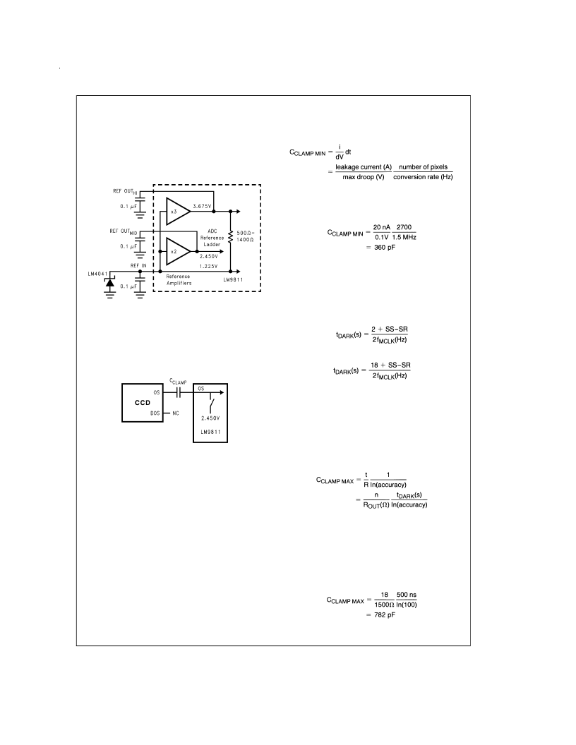
4.2 Clamp Capacitor Section
This section is very long because it is relatively complicated
to explain, but the answer is short and simple: A clamp ca-
pacitor value of 0.01 μF should work in almost all applica-
tions. The rest of this section describes exactly how this
value is selected.
The output signal of many CCDs rides on a large DC offset
(typically 8V to 10V) which is incompatible with the LM9811’s
5V operation. To eliminate this offset without resorting to ad-
ditional higher voltage components, the output of the CCD is
AC coupled to the LM9811 through a DC blocking capacitor,
C
(the CCD’s DOS output is not used). The value of
this capacitor is determined by the leakage current of the
LM9811’s OS input and the output impedance of the CCD.
The leakage through the OS input determines how quickly
the capacitor value will drift from the clamp value of REF
OUT
, which then determines how many pixels can be
processed before the droop causes errors in the conversion
(
±
0.1V is the recommended limit). The output impedance of
the CCD determines how quickly the capacitor can be
charged to the clamp value during the black reference period
at the beginning of every line.
The minimum clamp capacitor value is determined by the
maximum droop the LM9811 can tolerate while converting
one CCD line. The following equation takes the maximum
leakage current into the OS input, the maximum allowable
droop (100 mV), the number of pixels on the CCD, and the
pixel conversion rate (f
MCLK
/8) and provides the minimum
clamp capacitor value:
For example, if the OS input leakage current is 20 nA worst-
case, the CCD has 2700 active pixels, the conversion rate is
1.5MHz (f
= 12MHz), and the max droop desired is
0.1V, the minimum clamp capacitor value is:
The maximum size of the clamp capacitor is determined by
the amount of time available to charge it to the desired value
during the optical black portion of the CCD output. The inter-
nal clamp is on for each pixel from the rising edge of the S/H
ref pulse to the falling edge of the S/H signal pulse (see Fig-
ures 7, 8). This time can be calculated using the values
stored in the Sample Signal and Sample Reference configu-
ration registers and the MCLK frequency. For normal CCDs:
And for even/odd CCDs:
Where SS is the value in the Sample Signal Position register
(0–15), SR is the value in the Sample Reference Position
register (0–14), f
is the MCLK frequency, and t
DARK
is
the amount of time (per pixel) that the clamp is on.
The following equation takes the number of optical black pix-
els, the amount of time (per pixel) that the clamp is closed,
the CCD’s output impedance, and the desired accuracy of
the final clamp voltage and provides the maximum clamp ca-
pacitor value that allows the clamp capacitor to settle to the
desired accuracy within a single line:
Where n = the number of optical black pixels, t
DARK
is the
amount of time (per pixel) that the clamp is on, R
is the
output impedance of the CCD, and accuracy is the ratio of
the worst-case initial capacitor voltage to the desired final
capacitor voltage. For example, if a CCD has 18 black refer-
ence pixels, the output impedance of the CCD is 1500
, the
LM9811 is configured to clamp for 500ns, the worst case ini-
tial voltage across the capacitor is 10V, and the desired volt-
age after clamping is 0.1V (accuracy = 10/0.1 = 100), then:
DS012813-29
FIGURE 21. Voltage Reference Generation
DS012813-30
FIGURE 22. OS Clamp Capacitor and Internal Clamp
www.national.com
23
相關(guān)PDF資料 |
PDF描述 |
|---|---|
| LM9811 | 10-Bit Greyscale/30-Bit Color Linear CCD Sensor Processor |
| LM9811CCV | 10-Bit Greyscale/30-Bit Color Linear CCD Sensor Processor |
| LM9831CCVJD | LM9831 42-Bit Color, 1200dpi USB Image Scanner |
| LM9831 | LM9831 42-Bit Color, 1200dpi USB Image Scanner |
| LM9831CCVJDX | LM9831 42-Bit Color, 1200dpi USB Image Scanner |
相關(guān)代理商/技術(shù)參數(shù) |
參數(shù)描述 |
|---|---|
| LM9812 | 制造商:NSC 制造商全稱:National Semiconductor 功能描述:LM9812 30-Bit Color Linear CCD Sensor Processor |
| LM9812CCV | 制造商:NSC 制造商全稱:National Semiconductor 功能描述:LM9812 30-Bit Color Linear CCD Sensor Processor |
| LM981-SC36 | 功能描述:基本/快動開關(guān) Foot Switch RoHS:否 制造商:Omron Electronics 觸點形式:SPDT 執(zhí)行器:Lever 電流額定值:5 A 電壓額定值 AC:250 V 電壓額定值 DC:30 V 功率額定值: 工作力:120 g IP 等級:IP 67 NEMA 額定值: 端接類型:Wire 安裝:Panel |
| LM981-ZZ | 功能描述:基本/快動開關(guān) Foot Switch RoHS:否 制造商:Omron Electronics 觸點形式:SPDT 執(zhí)行器:Lever 電流額定值:5 A 電壓額定值 AC:250 V 電壓額定值 DC:30 V 功率額定值: 工作力:120 g IP 等級:IP 67 NEMA 額定值: 端接類型:Wire 安裝:Panel |
| LM981-ZZ-1 | 功能描述:基本/快動開關(guān) Foot Switch RoHS:否 制造商:Omron Electronics 觸點形式:SPDT 執(zhí)行器:Lever 電流額定值:5 A 電壓額定值 AC:250 V 電壓額定值 DC:30 V 功率額定值: 工作力:120 g IP 等級:IP 67 NEMA 額定值: 端接類型:Wire 安裝:Panel |
發(fā)布緊急采購,3分鐘左右您將得到回復(fù)。