- 您現在的位置:買賣IC網 > PDF目錄361044 > LMX2434 (National Semiconductor Corporation) PLLatinum Dual High Frequency Synthesizer for RF Personal Communications PDF資料下載
參數資料
| 型號: | LMX2434 |
| 廠商: | National Semiconductor Corporation |
| 英文描述: | PLLatinum Dual High Frequency Synthesizer for RF Personal Communications |
| 中文描述: | PLLatinum雙高頻率合成射頻個人通信 |
| 文件頁數: | 29/49頁 |
| 文件大小: | 943K |
| 代理商: | LMX2434 |
第1頁第2頁第3頁第4頁第5頁第6頁第7頁第8頁第9頁第10頁第11頁第12頁第13頁第14頁第15頁第16頁第17頁第18頁第19頁第20頁第21頁第22頁第23頁第24頁第25頁第26頁第27頁第28頁當前第29頁第30頁第31頁第32頁第33頁第34頁第35頁第36頁第37頁第38頁第39頁第40頁第41頁第42頁第43頁第44頁第45頁第46頁第47頁第48頁第49頁
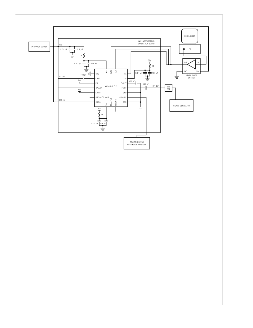
LMX243x Charge Pump Test Setup
20053588
The block diagram above illustrates the setup required to
measure the LMX243x device’s RF charge pump sink cur-
rent. The same setup is used for the LMX2430TM Evaluation
Board. The purpose of this test is to assess the functionality
of the RF charge pump. The IF charge pump is evaluated in
the same way.
This setup uses an open loop configuration. A power supply
is connected to Vcc. By means of a signal generator, a 10
MHz signal is typically applied to the FinRF pin. The signal is
one of two inputs to the phase/ frequency detector (PFD).
The 3 dB pad provides a 50
match between the PLL and
the signal generator. The OSCin pin is tied to Vcc. This
establishes the other input to the PFD. Alternatively, this
input can be tied directly to the ground plane. The EN and
ENosc pins are also both tied to Vcc. A Semiconductor
Parameter Analyzer is connected to the CPoutRF pin and
used to measure the sink, source, and TRI-STATE leakage
currents.
Let F
r
represent the frequency of the signal applied to the
OSCin pin, which is simply zero in this case (DC), and let F
p
represent the frequency of the signal applied to the FinRF
pin. The PFD is sensitive to the rising edges of F
and F
p
.
Assuming positive VCO characteristics (RF_CPP bit = 1);
the charge pump turns ON, and sinks current when the first
rising edge of F
is detected. Since F
has no rising edge, the
charge pump continues to sink current indefinitely. In order
to measure the RF charge pump source current, the
RF_CPP bit is simply set to 0 (negative VCO characteristics)
in CodeLoader. Similarly, in order to measure the TRI-STATE
leakage current, the RF_CPT bit is set to 1.
The measurements are typically taken over supply voltage
and temperature. The measurements are also typically taken
at the HIGH and LOW charge pump current gains. The
charge pump current gain can be controlled by the RF_CPG
bit in CodeLoader. Once the charge pump currents are
determined, the (i) charge pump output current magnitude
variation versus charge pump output voltage, (ii) charge
pump output sink current versus charge pump output source
current mismatch, and (iii) charge pump output current mag-
nitude versus tempeature, can be calculated. Refer to the
Charge Pump Current Specifications Definition
for more
details.
L
www.national.com
29
相關PDF資料 |
PDF描述 |
|---|---|
| LMX2434TM | PLLatinum Dual High Frequency Synthesizer for RF Personal Communications |
| LMX2434TMX | PLLatinum Dual High Frequency Synthesizer for RF Personal Communications |
| LMX2430SLEX | PLLatinum Dual High Frequency Synthesizer for RF Personal Communications |
| LMX2430TM | PLLatinum Dual High Frequency Synthesizer for RF Personal Communications |
| LMX2430TMX | PLLatinum Dual High Frequency Synthesizer for RF Personal Communications |
相關代理商/技術參數 |
參數描述 |
|---|---|
| LMX2434EVAL | 功能描述:時鐘和定時器開發工具 LMX2434 EVAL BOARD RoHS:否 制造商:Texas Instruments 產品:Evaluation Modules 類型:Clock Conditioners 工具用于評估:LMK04100B 頻率:122.8 MHz 工作電源電壓:3.3 V |
| LMX2434EVAL/NOPB | 功能描述:時鐘和定時器開發工具 LMX2434 EVAL BOARD RoHS:否 制造商:Texas Instruments 產品:Evaluation Modules 類型:Clock Conditioners 工具用于評估:LMK04100B 頻率:122.8 MHz 工作電源電壓:3.3 V |
| LMX2434SLEX | 制造商:Texas Instruments 功能描述:PLL Frequency Synthesizer Dual 500MHz to 5000MHz 20-Pin LAM UCSP T/R |
| LMX2434SLEX/NOPB | 功能描述:鎖相環 - PLL RoHS:否 制造商:Silicon Labs 類型:PLL Clock Multiplier 電路數量:1 最大輸入頻率:710 MHz 最小輸入頻率:0.002 MHz 輸出頻率范圍:0.002 MHz to 808 MHz 電源電壓-最大:3.63 V 電源電壓-最小:1.71 V 最大工作溫度:+ 85 C 最小工作溫度:- 40 C 封裝 / 箱體:QFN-36 封裝:Tray |
| LMX2434TM | 制造商:Texas Instruments 功能描述:PLL Frequency Synthesizer Dual 500MHz to 5000MHz 20-Pin TSSOP Rail |
發布緊急采購,3分鐘左右您將得到回復。