- 您現在的位置:買賣IC網 > PDF目錄361045 > LPC662IM (NATIONAL SEMICONDUCTOR CORP) Low Power CMOS Dual Operational Amplifier PDF資料下載
參數資料
| 型號: | LPC662IM |
| 廠商: | NATIONAL SEMICONDUCTOR CORP |
| 元件分類: | 運算放大器 |
| 英文描述: | Low Power CMOS Dual Operational Amplifier |
| 中文描述: | DUAL OP-AMP, 6300 uV OFFSET-MAX, 0.35 MHz BAND WIDTH, PDSO8 |
| 封裝: | SO-8 |
| 文件頁數: | 7/16頁 |
| 文件大小: | 585K |
| 代理商: | LPC662IM |
Typical Performance Characteristics
V
S
=
±
7.5V, T
A
= 25C unless otherwise specified (Continued)
Application Hints
AMPLIFIER TOPOLOGY
The topology chosen for the LPC662 is unconventional
(compared to general-purpose op amps) in that the tradi-
tional unity-gain buffer output stage is not used; instead, the
output is taken directly from the output of the integrator, to al-
low rail-to-rail output swing. Since the buffer traditionally de-
livers the power to the load, while maintaining high op amp
gain and stability, and must withstand shorts to either rail,
these tasks now fall to the integrator.
As a result of these demands, the integrator is a compound
affair with an embedded gain stage that is doubly fed forward
(via C
and C
) by a dedicated unity-gain compensation
driver. In addition, the output portion of the integrator is a
push-pull configuration for delivering heavy loads. While
sinking current the whole amplifier path consists of three
gain stages with one stage fed forward, whereas while
sourcing the path contains four gain stages with two fed
forward.
The large signal voltage gain while sourcing is comparable
to traditional bipolar op amps for load resistance of at least
5 k
. The gain while sinking is higher than most CMOS op
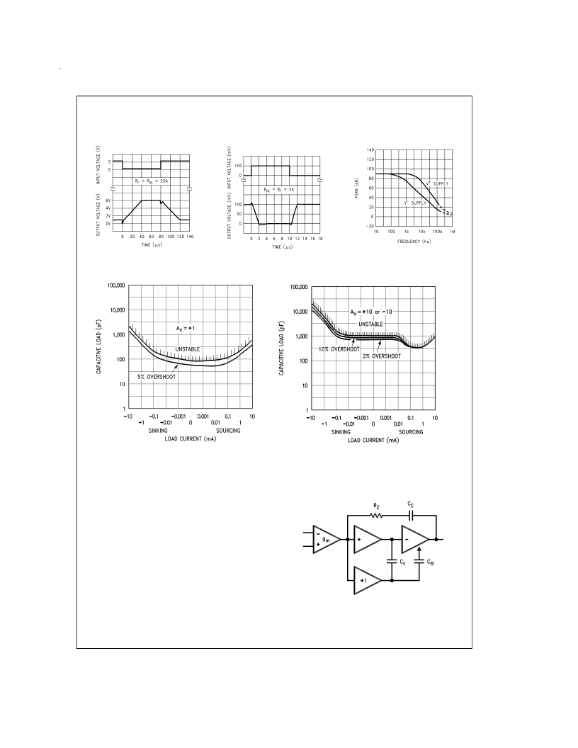
Inverting Large-Signal
Pulse Response
DS010548-47
Inverting Small-Signal
Pulse Response
DS010548-48
Power Supply Rejection
Ratio vs Frequency
DS010548-37
Stability vs Capacitive Load
DS010548-4
Avoid resistive loads of less than 500
, as they may cause
Note:
Stability vs Capacitive Load
DS010548-5
DS010548-6
FIGURE 1. LPC662 Circuit Topology (Each Amplifier)
www.national.com
7
相關PDF資料 |
PDF描述 |
|---|---|
| LPC662IN | Low Power CMOS Dual Operational Amplifier |
| LQA28A | 3V, 1W Boosted Boomer |
| LV8572A | LV8572A Low Voltage Real Time Clock (RTC) |
| LV8572AM | LV8572A Low Voltage Real Time Clock (RTC) |
| LV8572AN | LV8572A Low Voltage Real Time Clock (RTC) |
相關代理商/技術參數 |
參數描述 |
|---|---|
| LPC662IM | 制造商:Texas Instruments 功能描述:OP AMP DUAL CMOS SMD SOIC8 662 |
| LPC662IM/NOPB | 功能描述:運算放大器 - 運放 RoHS:否 制造商:STMicroelectronics 通道數量:4 共模抑制比(最小值):63 dB 輸入補償電壓:1 mV 輸入偏流(最大值):10 pA 工作電源電壓:2.7 V to 5.5 V 安裝風格:SMD/SMT 封裝 / 箱體:QFN-16 轉換速度:0.89 V/us 關閉:No 輸出電流:55 mA 最大工作溫度:+ 125 C 封裝:Reel |
| LPC662IMX | 功能描述:運算放大器 - 運放 RoHS:否 制造商:STMicroelectronics 通道數量:4 共模抑制比(最小值):63 dB 輸入補償電壓:1 mV 輸入偏流(最大值):10 pA 工作電源電壓:2.7 V to 5.5 V 安裝風格:SMD/SMT 封裝 / 箱體:QFN-16 轉換速度:0.89 V/us 關閉:No 輸出電流:55 mA 最大工作溫度:+ 125 C 封裝:Reel |
| LPC662IMX/NOPB | 功能描述:運算放大器 - 運放 RoHS:否 制造商:STMicroelectronics 通道數量:4 共模抑制比(最小值):63 dB 輸入補償電壓:1 mV 輸入偏流(最大值):10 pA 工作電源電壓:2.7 V to 5.5 V 安裝風格:SMD/SMT 封裝 / 箱體:QFN-16 轉換速度:0.89 V/us 關閉:No 輸出電流:55 mA 最大工作溫度:+ 125 C 封裝:Reel |
| LPC662IN | 制造商:NSC 制造商全稱:National Semiconductor 功能描述:Low Power CMOS Dual Operational Amplifier |
發布緊急采購,3分鐘左右您將得到回復。