- 您現在的位置:買賣IC網 > Datasheet目錄41 > LTC3445EUF#TRPBF (Linear Technology)IC REG TRPL BUCK/LINEAR 24-QFN Datasheet資料下載
參數資料
| 型號: | LTC3445EUF#TRPBF |
| 廠商: | Linear Technology |
| 文件頁數: | 19/24頁 |
| 文件大小: | 475K |
| 描述: | IC REG TRPL BUCK/LINEAR 24-QFN |
| 標準包裝: | 2,500 |
| 拓撲: | 降壓(降壓)(1),線性(LDO)(2) |
| 功能: | 任何功能 |
| 輸出數: | 3 |
| 頻率 - 開關: | 1.5MHz |
| 電壓/電流 - 輸出 1: | 0.85 V ~ 1.55 V,600mA |
| 電壓/電流 - 輸出 2: | 可調至0.6V,50mA |
| 電壓/電流 - 輸出 3: | 可調至0.6V,50mA |
| 帶 LED 驅動器: | 無 |
| 帶監控器: | 無 |
| 帶序列發生器: | 無 |
| 電源電壓: | 2.5 V ~ 5.5 V |
| 工作溫度: | -40°C ~ 85°C |
| 安裝類型: | 表面貼裝 |
| 封裝/外殼: | 24-WFQFN 裸露焊盤 |
| 供應商設備封裝: | 24-QFN 裸露焊盤(4x4) |
| 包裝: | 帶卷 (TR) |
19
LTC3445
3445fa
Checking Transient Response
The regulator loop response can be checked by looking at
the load transient response. Switching regulators take
several cycles to respond to a step in load current. When
a load step occurs, V
OUT
immediately shifts by an amount
equal to (I
LOAD
" ESR), where ESR is the effective series
resistance of C
OUT
. I
LOAD
also begins to charge or
discharge C
OUT
, which generates a feedback error signal.
The regulator loop then acts to return V
OUT
to its steady-
state value. During this recovery time V
OUT
can be moni-
tored for overshoot or ringing that would indicate a stability
problem. For a detailed explanation of switching control
loop theory, see Application Note 76.
A second, more severe transient is caused by switching in
loads with large (>1礔) supply bypass capacitors. The
discharged bypass capacitors are effectively put in parallel
with C
OUT
, causing a rapid drop in V
OUT
. No regulator can
deliver enough current to prevent this problem if the load
switch resistance is low and it is driven quickly. The only
solution is to limit the rise time of the switch drive so that
the load rise time is limited to approximately (25 " C
LOAD
).
Thus, a 10礔 capacitor charging to 3.3V would require a
250祍 rise time, limiting the charging current to about
130mA.
LDO REGULATORS
The LDOs in the LTC3445 are 50mA low dropout regula-
tors with low quiescent and shutdown currents. Each
device is capable of supplying 50mA at a dropout voltage
of 300mV. The LDOs are current limited to greater than
50mA but less than 75mA. The output voltages of the
LDOs are set with external resistive dividers according to
the following formula:
V
LDOOUT1
= 0.6(1 + R1/R2)
(4)
V
LDOOUT2
= 0.6(1 + R3/R4)
(5)
Output Capacitance and Transient Response
The LTC3445 LDOs are designed to be stable with a wide
range of output capacitors. A minimum output capacitor
of 2.2礔 with an ESR of 3& or less is recommended to
internal power MOSFET switches. Each time the gate is
switched from high to low to high again, a packet of
charge, dQ, moves from V
CC1
to ground. The resulting
dQ/dt is the current out of V
CC1
that is typically larger
than the DC bias current. In continuous mode, I
GATECHG
= f(Q
T
+ Q
B
) where Q
T
and Q
B
are the gate charges of the
internal top and bottom switches. Both the DC bias and
gate charge losses are proportional to V
CC1
and thus
their effects will be more pronounced at higher supply
voltages.
2. I
2
R losses are calculated from the resistances of the
internal switches, R
SW
, and external inductor R
L
. In
continuous mode, the average output current flowing
through inductor L is
chopped
between the main
switch and the synchronous switch. Thus, the series
resistance looking into the SW pin is a function of both
top and bottom MOSFET R
DS(ON)
and the duty cycle
(DC) as follows:
R
SW
= (R
DS(ON)TOP
)(DC) + (R
DS(ON)BOT
)(1 DC)
The R
DS(ON)
for both the top and bottom MOSFETs can
be obtained from the Typical Performance Charateristics
curves. Thus, to obtain I
2
R losses, simply add R
SW
to
R
L
and multiply the result by the square of the average
output current.
Other losses including C
IN
and C
OUT
ESR dissipative
losses and inductor core losses generally account for
less than 2% total additional loss.
APPLICATIO S I FOR ATIO
U
U
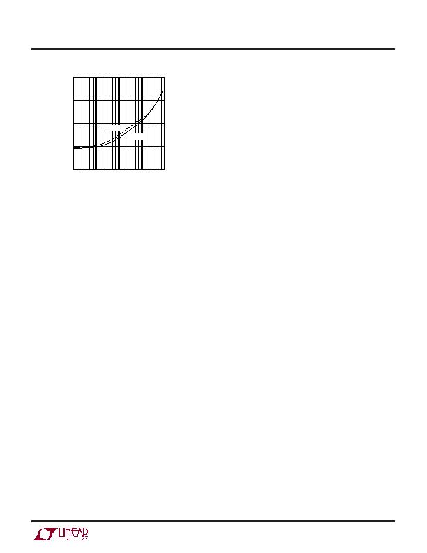
U
Figure 8. Power Loss vs Load Current, V
CC1
= 3.6V
LOAD CURRENT (mA)
1
10
100
1000
0.1
10
100 1000
3445 F08
0.1
1
DAC MIN
DAC MAX
相關PDF資料 |
PDF描述 |
|---|---|
| LTC3446IDE#PBF | IC REG TRPL BCK/LINEAR 14-DFN |
| LTC3537EUD#TRPBF | IC REG DL BST/LINEAR SYNC 16-QFN |
| LTC3541EDD#TRPBF | IC REG DL BCK/LINEAR SYNC 10-DFN |
| LTC3670EDDB#TRPBF | IC REG TRPL BCK/LINEAR 12DFN |
| LTC3672BEDC-1#TRPBF | IC REG TRPL BCK/LINEAR 8-DFN |
相關代理商/技術參數 |
參數描述 |
|---|---|
| LTC3446 | 制造商:LINER 制造商全稱:Linear Technology 功能描述:Monolithic Buck Regulator with Dual VLDO Regulators |
| LTC3446EDE | 制造商:LINER 制造商全稱:Linear Technology 功能描述:Monolithic Buck Regulator with Dual VLDO Regulators |
| LTC3446EDE#PBF | 功能描述:IC REG TRPL BCK/LINEAR 14-DFN RoHS:是 類別:集成電路 (IC) >> PMIC - 穩壓器 - 線性 + 切換式 系列:- 標準包裝:2,500 系列:- 拓撲:降壓(降壓)同步(3),線性(LDO)(2) 功能:任何功能 輸出數:5 頻率 - 開關:300kHz 電壓/電流 - 輸出 1:控制器 電壓/電流 - 輸出 2:控制器 電壓/電流 - 輸出 3:控制器 帶 LED 驅動器:無 帶監控器:無 帶序列發生器:是 電源電壓:5.6 V ~ 24 V 工作溫度:-40°C ~ 85°C 安裝類型:* 封裝/外殼:* 供應商設備封裝:* 包裝:* |
| LTC3446EDE#TRPBF | 功能描述:IC REG TRPL BCK/LINEAR 14-DFN RoHS:是 類別:集成電路 (IC) >> PMIC - 穩壓器 - 線性 + 切換式 系列:- 標準包裝:2,500 系列:- 拓撲:降壓(降壓)同步(3),線性(LDO)(2) 功能:任何功能 輸出數:5 頻率 - 開關:300kHz 電壓/電流 - 輸出 1:控制器 電壓/電流 - 輸出 2:控制器 電壓/電流 - 輸出 3:控制器 帶 LED 驅動器:無 帶監控器:無 帶序列發生器:是 電源電壓:5.6 V ~ 24 V 工作溫度:-40°C ~ 85°C 安裝類型:* 封裝/外殼:* 供應商設備封裝:* 包裝:* |
| LTC3446EDE-PBF | 制造商:LINER 制造商全稱:Linear Technology 功能描述:Monolithic Buck Regulator with Dual VLDO Regulators |
發布緊急采購,3分鐘左右您將得到回復。