- 您現(xiàn)在的位置:買賣IC網(wǎng) > Datasheet目錄42 > LTC4212IMS#TRPBF (Linear Technology)IC CTRLR HOTSWAP TIMEOUT 10MSOP Datasheet資料下載
參數(shù)資料
| 型號: | LTC4212IMS#TRPBF |
| 廠商: | Linear Technology |
| 文件頁數(shù): | 21/24頁 |
| 文件大小: | 234K |
| 描述: | IC CTRLR HOTSWAP TIMEOUT 10MSOP |
| 標準包裝: | 2,500 |
| 類型: | 熱交換控制器 |
| 應(yīng)用: | 通用 |
| 內(nèi)部開關(guān): | 無 |
| 電源電壓: | 2.5 V ~ 16.5 V |
| 工作溫度: | -40°C ~ 85°C |
| 安裝類型: | 表面貼裝 |
| 封裝/外殼: | 10-TFSOP,10-MSOP(0.118",3.00mm 寬) |
| 供應(yīng)商設(shè)備封裝: | 10-MSOP |
| 包裝: | 帶卷 (TR) |
21
LTC4212
4212f
OPERATIO
For example:
If a sense resistor with 7m& ?% R
TOL
is used for current
limiting, the nominal trip current I
TRIP(NOM)
= 7.1A. From
Equations 11 and 12, I
TRIP(MIN)
= 5.4A and I
TRIP(MAX)
=
9.02A respectively.
For proper operation and to avoid the circuit breaker
tripping unnecessarily, the minimum trip current
(I
TRIP(MIN)
) must exceed the circuits maximum operating
load current. For reliability purposes, the operation at the
maximum trip current (I
TRIP(MAX)
) must be evaluated
carefully. If necessary, two resistors with the same R
TOL
can be connected in parallel to yield an R
SENSE(NOM)
value
that fits the circuit requirements.
Power MOSFET Selection Criteria
To start the power MOSFET selection process, choose the
maximum drain-to-source voltage, V
DS(MAX)
, and the
maximum drain current, I
D(MAX)
of the MOSFET. The
V
DS(MAX)
rating must exceed the maximum input supply
voltage (including surges, spikes, ringing, etc.) and the
I
D(MAX)
rating must exceed the maximum short-circuit
current in the system during a fault condition. In addition,
consider three other key parameters: 1) the required gate-
source (V
GS
) voltage drive, 2) the voltage drop across the
drain-to-source on resistance, R
DS(ON)
and 3) the maxi-
mum junction temperature rating of the MOSFET.
Power MOSFETs are classified into two categories: stan-
dard MOSFETs (R
DS(ON)
specified at V
GS
= 10V) and
logic-level MOSFETs (R
DS(ON)
specified at V
GS
= 5V). The
absolute maximum rating for V
GS
is typically ?0V for
standard MOSFETs. However, the V
GS
maximum rating
for logic-level MOSFETs ranges from ?V to ?0V de-
pending upon the manufacturer and the specific part
number. The LTC4212s GATE overdrive as a function of
V
CC
is illustrated in the Typical Performance curves. Logic-
level MOSFETs are recommended for low supply voltage
applications and standard MOSFETs can be used for appli-
cations where supply voltage is greater than 4.75V.
Note that in some applications, the gate of the external
MOSFET can discharge faster than the output voltage
when the circuit breaker is tripped. This causes a negative
V
GS
voltage on the external MOSFET. Usually, the selected
external MOSFET should have a 盫
GS(MAX)
rating that is
higher than the operating input supply voltage to ensure
that the external MOSFET is not destroyed by a negative
V
GS
voltage. In addition, the 盫
GS(MAX)
rating of the
MOSFET must be higher than the gate overdrive voltage.
Lower 盫
GS(MAX)
rating MOSFETs can be used with the
LTC4212 if the GATE overdrive is clamped to a lower
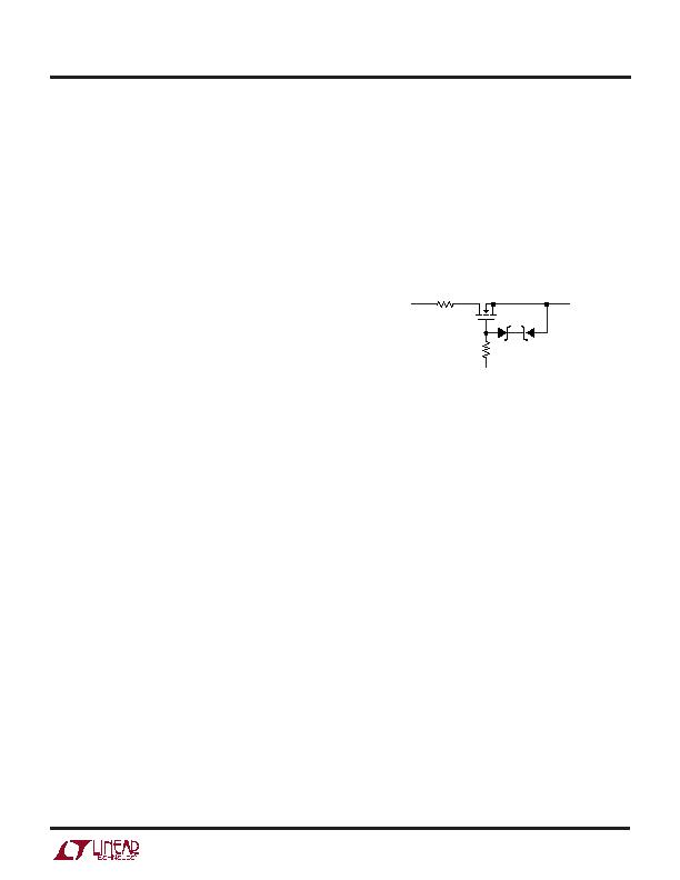
voltage. The circuit in Figure 8 illustrates the use of zener
diodes to clamp the LTC4212s GATE overdrive signal if
lower voltage MOSFETs are used.
V
CC
V
OUT
*USER SELECTED VOLTAGE CLAMP
(A LOW BIAS CURRENT ZENER DIODE IS RECOMMENDED)
1N4688 (5V)
1N4692 (7V): LOGIC-LEVEL MOSFET
1N4695 (9V)
1N4702 (15V): STANDARD-LEVEL MOSFET
4212 F08
R
SENSE
GATE
D2*
D1*
Q1
R
G
200&
Figure 8. Optional Gate Clamp for Lower V
GS(MAX)
MOSFETs
The R
DS(ON)
of the external pass transistor should be low
to make its drain-source voltage (V
DS
) a small percentage
of V
CC
. At a V
CC
= 2.5V, V
DS
+ V
RSENSE
= 0.1V yields 4%
error at the output voltage. This restricts the choice of
MOSFETs to very low R
DS(ON)
. At higher V
CC
voltages, the
V
DS
requirement can be relaxed in which case MOSFET
package dissipation (P
D
and T
J
) may limit the value of
R
DS(ON)
. Table 6 lists some power MOSFETs that can be
used with the LTC4212.
For reliable circuit operation, the maximum junction tem-
perature (T
J(MAX)
) for a power MOSFET should not exceed
the manufacturers recommended value. This includes
normal mode operation, start-up, current-limit and
autoretry mode in a fault condition. Under normal condi-
tions the junction temperature of a power MOSFET is given
by Equation 13:
MOSFET Junction Temperature,
T
J(MAX)
d T
A(MAX)
+ ?/DIV>
JA
" P
D
(13)
相關(guān)PDF資料 |
PDF描述 |
|---|---|
| LTC4214-1IMS#TRPBF | IC CTRLR HOTSWAP NEGVOLT 10MSOP |
| LTC4215IUFD#PBF | IC CNTRLR HOT SWAP 24-QFN |
| LTC4216IDE#TRPBF | IC CNTRLR HOT SWAP 12-DFN |
| LTC4221IGN#TRPBF | IC CTRLR HOTSWAP DUAL 16SSOP |
| LTC4222CG#PBF | IC CTRLR DUAL HOT SWAP 36-SSOP |
相關(guān)代理商/技術(shù)參數(shù) |
參數(shù)描述 |
|---|---|
| LTC4213 | 制造商:LINER 制造商全稱:Linear Technology 功能描述:No RSENSE? Electronic Circuit Breaker |
| LTC4213CDDB | 制造商:LINER 制造商全稱:Linear Technology 功能描述:No RSENSE? Electronic Circuit Breaker |
| LTC4213CDDB#PBF | 制造商:Linear Technology 功能描述:Hot Swap Controller 1-CH 6V 8-Pin DFN EP 制造商:Linear Technology 功能描述:HOT SWAP CNTRL 6V INT SW 8DFN 制造商:Linear Technology 功能描述:HOT SWAP CNTRL, 6V, INT SW, 8DFN |
| LTC4213CDDB#TRMPBF | 功能描述:IC CIRC BREAK ELEC 8-DFN RoHS:是 類別:集成電路 (IC) >> 專用 IC 系列:* 產(chǎn)品培訓(xùn)模塊:Lead (SnPb) Finish for COTS Obsolescence Mitigation Program 標準包裝:1 系列:- 類型:調(diào)幀器 應(yīng)用:數(shù)據(jù)傳輸 安裝類型:表面貼裝 封裝/外殼:400-BBGA 供應(yīng)商設(shè)備封裝:400-PBGA(27x27) 包裝:散裝 |
| LTC4213CDDB#TRPBF | 功能描述:IC CIRC BREAK ELEC 8-DFN RoHS:是 類別:集成電路 (IC) >> 專用 IC 系列:* 產(chǎn)品培訓(xùn)模塊:Lead (SnPb) Finish for COTS Obsolescence Mitigation Program 標準包裝:1 系列:- 類型:調(diào)幀器 應(yīng)用:數(shù)據(jù)傳輸 安裝類型:表面貼裝 封裝/外殼:400-BBGA 供應(yīng)商設(shè)備封裝:400-PBGA(27x27) 包裝:散裝 |
發(fā)布緊急采購,3分鐘左右您將得到回復(fù)。